Photovoltaic spectroscopic study of GaN epilayers and InGaN quantum well structures
- PDF / 107,288 Bytes
- 5 Pages / 612 x 792 pts (letter) Page_size
- 37 Downloads / 288 Views
MATERIALS RESEARCH
Welcome
Comments
Help
Photovoltaic spectroscopic study of GaN epilayers and InGaN quantum well structures W. Liu, M.F. Li, and K.L. Teo Center for Optoelectronics, Department of Electrical Engineering, The National University of Singapore, Singapore 119260
Nakao Akutsu and Koh Matsumoto Nippon Sanso Co., Tsukuba Laboratories, 10 Ohkubo Tsukuba, Ibaraki, 300-26, Japan (Received 19 August 1998; accepted 13 April 1999)
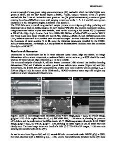
Room-temperature photovoltaic spectroscopy was applied to study undoped GaN, n-type GaN, and InGaN quantum well structures. Clear exciton absorption was observed in the photovoltaic spectra of the undoped GaN, and polarization measurements were made to identify the exciton absorption. For the n-type GaN sample, instead of the exciton absorption we observed only bulk absorption edge, which may be due to the free carrier screening effect. For the InGaN quantum well structures, the photovoltaic spectra showed relatively complicated line shape due to the overlap of the signals from different layers. By changing the reference phase of the lock-in amplifier, we were able to suppress some of the signals and thus identify the origin of the corresponding signal.
I. INTRODUCTION
The band gaps of GaN (3.4 eV) and related compound semiconductors such as InN (1.9 eV), AlN (6.2 eV), and their alloys, cover a wide spectral range from the red light to the ultraviolet (UV) region. In addition, they are all direct-band-gap semiconductors and have very high radiative recombination efficiency.1 Moreover, they are believed to be quite tolerant of elevated temperatures and caustic environments. Finally, an electron saturation velocity of 3 × 107 cm/s was predicted for GaN.2,3 Therefore, with these advantages, they have been viewed as the most promising candidates for fabricating UV–blue light-emitting devices and high-power electronic devices, and they have attracted more and more attention1–3 in recent years. The UV–blue light-emitting devices will make the full color display possible, and the UV–blue laser diodes will increase the CD-ROM storage density significantly. The electronic devices based on GaN will find their application in the field of aerospace and power engineering. GaN-based blue light-emitting diodes have already been commercialized4 and rapid progress on GaN-based blue light laser diodes has been made by Nakamura et al.5 With respect to electronic devices, AlGaN–GaN single heterostructure modulation doped field effect transistors (MODFET) with a maximum oscillation frequency of more than 70 GHz have also been fabricated.6 Despite these significant achievements, the quality of the materials is far from perfect. Appropriate substrates with lattice constants and thermal expansion coefficients close to GaN have not been found 2794
http://journals.cambridge.org
J. Mater. Res., Vol. 14, No. 7, Jul 1999 Downloaded: 13 Mar 2015
and most growth processes are based on heteroepitaxy, with substrate properties quite different from those of the epilayers. This results in a large strain in t
Data Loading...