Plasma Stimulated Growth of InP from TEL and PH 3
- PDF / 405,076 Bytes
- 8 Pages / 420.48 x 639 pts Page_size
- 65 Downloads / 254 Views
PLASMA STIMULATED GROWTH OF InP FROM TEl AND PH3 H. REINECKE, F. GRAFAHREND, A. BRAUERS, H. LUTH AND P. Institute of Semiconductor Electronics and II. Physikalisches Institut, Technical University Aachen, D-5100 Aachen, FRG
BALK
ABSTRACT This study describes the application of a dc-plasma to stimulate growth of InP in a MOCVD system using In(C 2 H5 ) 3 and PH 3 . Precracking of PH3 enables a substantial reduction of the growth temperature to well below 500 K. In addition, at temperatures where InP is commonly deposited ýv870 K) a significant lowering of the V/Ill input ratio is possible. The fact that InP is relatively insensitive to low energy ion bombardement permits deposition in a canal ray configuration.
1. INTRODUCTION The deposition of semiconductor films at low growth temperatures and low total pressures is an important technological aim since it reduces dopant diffusion in layered structures and permits sharper compositional transistions. However, at these conditions the rate of growth is affected by strong kinetic limitations. This was shown in dejail for the growth of GaAs using MOCVD [L-3J . At total pressures below 10 Pa the thermal decomposition of the hydride (AsH 3 for the growth of GaAs, PH 3 for the growth of InP) is significantly reduced. An acceleration of the growth process in the temperature region where kinetic control dominates the growth process is possible by external stimulation, for example by UV irradiation or by a plasma. Plasma stimulated growth of GaAs from evaporated elemental Ga and As (between 620 and 770 K) was reported by Hariu [43. Shimizu investigated ion beam epitaxy of GaAs (from 490 to 820 K) and InP (from 480 to 690 K) [ýJ.Segui deposited amorphous GaAs from Ga (CH 3 ) 3 (TMG) and AsH 3 using a low frequency low power discharge [6). Pande used the same starting materials for the plasma assisted growth of monocrystalline GaAs films E[7. In our laboratory we investigated the dc-plasma stimulated MOCVD growth of GaAs and compared Ga(CH 3 ) 3 and Ga(C 2 H5 ) 3 (TEG) as Ga sources[8,9j. We also reported that dc-plasma precracking of PH3 during InP epitaxy permits a substantial reduction of the phosphine pressure or the lowering of the deposition temperature (< 750 K) (92. Recently Sakai et al. C10] presented data on the growth of InP in the temperature range from 570 K to 870 K with an r.f. plasma (13.56 MHz) used to precrack the PH3 . The study described in the present paper was concerned with the deposition of InP from TEl and PH 3 using a dc plasma system in the canal ray configuration. This arrangement permits the introduction of a controlled ion beam into the substrate zone. We compare the results on deposition rate and film properties obtained with plasma to results for deposition without plasma stimulation.
II.
EXPERIMENTAL
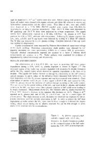
The MOCVD plasma apparatus (fig. 1) used in this study is the same as that employed for the plasma stimulated growth of GaAs; in the present work we used TEL and PH3 in a H2 carrier as starting materials. All data presented in this paper were ob
Data Loading...