Plasma Synthesis of Rare Earth Doped Integrated Optical Waveguides
- PDF / 2,185,110 Bytes
- 6 Pages / 414.72 x 648 pts Page_size
- 94 Downloads / 339 Views
INTRODUCTION The monolithic integration of electronic and photonic devices onto a single chip has become the focus of considerable research effort worldwide in recent years 1, 2. Advances in these optoelectronic integrated circuits, or OEICs, are driven by the needs of second-generation photonic systems including optical interconnects, optical computing, signal processing and communications. This new technology has the potential to boost considerably the sophistication and performance of existing and proposed advanced photonic systems. Future components will be capable of sending information at data rates greater than 10 Gbits/sec, with highly parallel
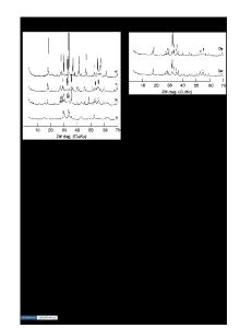
architecture and low power consumption. Key research and development concerns include both materials design and processing issues. Optoelectronic integrated circuits combine devices that implement optical functions in a guided wave structure with electronic semiconductor devices formed on the same substrate. The electronics of such components is now well mastered, and the next challenge is the development of the optical functions, which are based either on semiconductor materials (SC quantum wells) or on dielectric waveguide structures. Our interest is in the latter. Dielectric waveguide structures are based on multilayer thin film technology. A sandwich is formed in which the central guiding film is of higher refractive index than the surrounding material. Planar waveguides guide light in the vertical direction but provide no lateral confinement. For compatibility with optical fibers and for efficient modulation, strip waveguides are essential and have been fabricated by sputtering, epitaxial layers, ion implantation, ion exchange, and diffusion techniques combined with standard lithographic technology 3-9. The required geometry of the waveguide depends essentially on the guided wavelength and the difference of refractive indices in the guiding region and the cladding layer material 1 0,11 . Such optical waveguides are the basic structures leading to advanced OptoElectronic Integrated Circuits or OEICs. By doping the guiding region with optically active impurities, integrated optical amplifiers and lasers can be fabricated. The principle is the same as for optical fiber amplifiers and lasers. However, multilayer-thin-film technologies allow the formation of waveguides with higher refractive index differences between the guiding region and the surrounding, and the optimum concentration of active optical centers can also be two orders of magnitude greater when incorporated in dielectric waveguide materials 12 . Consequently the typical size of an 241 Mat. Res. Soc. Symp. Proc. Vol. 392 @1995 Materials Research Society
integrated amplifier/laser device is about 1 cm, of tolmmake as is typical for optical fiber lasers. By using spiral-strip waveguides it could be instead possible high performance integrated devices. An important application for such active OEICs is the fabrication of 1.53 p~m lasers by doping the waveguide with Er 3 + ions. Importantly, note that the
Data Loading...