Porous Silicon Oxynitride Films Derived from Polysilazane as a Novel Low-Dielectric Constant Material
- PDF / 1,789,190 Bytes
- 6 Pages / 417.6 x 639 pts Page_size
- 48 Downloads / 350 Views
Mat. Res. Soc. Symp. Proc. Vol. 565 01999 Materials Research Society
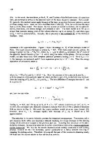
oxidation of perhydropolysilazane after of Polysilazaneand x...Miture PPSZ Precursor Solution SFoamingAgent pre-baking, and the acrylic polymer works as a foaming agent for producing a Deposition porous structure after curing. Figure 1 shows the process flow for ..EvaporatePartsof Foaming Prebake on Hotplate obtaining porous silica films from PPSZ SAgent precursor solution. After depositing the PPSZ solution on substrates by spin N2 Furnace Cure ... Evaporat all Foaming Agent coating, samples were placed on hot plates in a common clean-room ambient (20-240C, 40-60%RH) for pre-baking at Thin Film PorousDielectric PPSZ 150'C(3min), 2200C(3min), and 3009C (3min), consecutively. After pre-baking, Figure 1. Process flow for PPSZ film samples were cured in an N2 ambient at formation. 400'C for 30min. The total time for the processing of thin porous films from the deposition of the precursor was about 1 hour. Film Characterization Samples for IR spectroscopy were prepared on IR-grade silicon wafers. IR spectra were obtained using Perkin Elmer's Paragon 1000. The cross-sectional SEM images were obtained using Hitachi's FE-SEM S-800. TDS (Thermal Desorption Spectroscopy) analysis was carried out upon heating from room temperature to 800tC at a heating rate of 1VC/sec in vacuum. The dielectric constants were measured by using a mercury probe electrode attached to a MOS capacitor structure (Al-gate metal/PPSZ film/thermal SiO 2 (600A)/n-Si) at a frequency of 100kHz. The adhesion of the film was investigated with a tape test according to ASTM D3359. RESULTS AND DISCUSSION Structural Characterizations The cross-sectional SEM images of PPSZ cured films (Figure 2) show the aggregation of granules with diameters ranging from 5 to 30 nm. These porous structures are formed during the curing process as a result of the vaporization of the acrylic polymer. The volume of
pores in the film can be varied widely by varying the content of the acrylic polymer in PPSZ solution. Figure 2(B) shows the good gapfill property of the film in the 0.20 jim gaps.
_.M" i
P B) A '4.
PPSZ (6000 A)
Vi
Si wafer
Figure 2. Cross-sectional SEM images of cured PPSZ film: (A) on bare silicon, (B) in 0.20 u m gaps.
42
ABS
4000
3500
3000
2500
2000
1500
1000
500
Figure 3. IR spectra of a PPSZ film as cured (A) and after standing in a clean room ambient for (B) 1 week, (C)30days, and (D) 60days. The clean room ambient was 20249C, 40-60%RH. FT-IR spectra of a typical PPSZ film just after curing at 400°C(in N2 ambient) are shown in Figure 3(A). The spectra show absorption peaks due to Si-H (830 cm-, 2,250 cm-'), Si-H 2 (960 cm', 980 cm', and 2,180 cm-), Si-O (1,070 cm') and Si-N (950 cm') moieties. The SiN moiety in the FT-IR spectra overlaps with the large Si-O absorption. However, neither absorbed water (-3,700cm') nor N-H (-3,350cm') peaks were observed. The atomic composition of the film by XPS analysis was Si/O/N/C = 40/55/5/0.5 (atomic %) which indicates that the PPSZ film h
Data Loading...