Position Control of Nucleation in Solid-Phase Crystallization of a-Si/SiO 2 by Ge Layer Insertion
- PDF / 149,495 Bytes
- 5 Pages / 612 x 792 pts (letter) Page_size
- 87 Downloads / 340 Views
V2.5.1
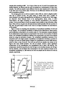
Position Control of Nucleation in Solid-Phase Crystallization of a-Si/SiO2 by Ge Layer Insertion Taizoh Sadoh, Kei Nagatomo, Isao Tsunoda, Atsushi Kenjo and Masanobu Miyao Department of Electronics, Kyushu University, Hakozaki, Fukuoka 812-8581, Japan ABSTRACT The effects of Ge layer insertion on the solid-phase crystallization (SPC) of a-Si on SiO2 have been investigated. Three types of sample structures, i.e., (a) a-Si/a-Ge/a-Si/SiO2, (b) a-Si/a-Ge/SiO2, and (c) SiO2/a-Ge/a-Si/SiO2, were prepared and annealed at 600oC. For the structure (a) with a thin (~ 5 nm) Ge layer, Ge atoms completely diffused into a-Si, and SPC was not enhanced. On the other hand, for the structure (a) with Ge layers thicker than 10 nm, Ge atoms were localized at the initial position. Such a localization of Ge atoms was remarkable for the structures (b) and (c) even for samples with thin Ge layers. For samples with Ge localization, significant enhancement of SPC of a-Si was observed. These results indicated that crystal nucleation was initiated in the inserted Ge layers, and then propagated into a-Si. The Ge layer insertion can be employed for positioning of crystal nucleation in SPC of a-Si.
INTRODUCTION Formation of high-quality polycrystalline Si (poly-Si) on glass substrates is a key technology for fabrication of high-performance thin-film transistors (TFTs) [1]. A melt-grown process such as laser annealing is widely used for this purpose. However, the grown surfaces become rough, because of the fluctuation of the laser power. Therefore, a technique for low-temperature (~550oC) solid-phase crystallization (SPC) is strongly required to realize completely flat surfaces, which is important for reduction of carrier scattering at the surfaces [2,3]. The SPC of amorphous Si (a-Si) on SiO2 consists of two processes, i.e., crystal nucleation and subsequent nucleus growth. The activation energies for these processes are 3.7 and 2.7 eV, respectively [4,5]. Due to the large activation energy (3.7 eV) for crystal nucleation, the SPC technique at a low temperature has not been established so far. In addition, nucleation occurs randomly in the entire region of a-Si films and at the a-Si/SiO2 interface. This makes the orientation control of crystal grains difficult. Consequently, low-temperature nucleation at a controlled position becomes essential for the fabrication of high-performance TFTs [6]. Our main idea to solve this problem is the Ge layer insertion into a-Si films to induce crystal nucleation in a selected region. In the present study, effects of Ge layer insertion into a-Si films on SPC have been investigated to enhance the nucleation at the a-Si/SiO2 interface. EXPERIMENTAL PROCEDURES Substrates used were n-type CZ-Si (100). They were thermally oxidized to grow SiO2 films
V2.5.2
(thickness: 160 nm). Subsequently, a-Ge and a-Si films (Ge thickness: 5-15 nm, total thickness: 50 nm) were deposited on SiO2 using a solid-source molecular beam epitaxy (MBE) system at room temperature (base pressure: 5x10-11 Torr). Three types of stac
Data Loading...