Preliminary Results on Large Area X-ray a-SiC:H Multilayer Detectors with Optically Addressed Readout
- PDF / 284,823 Bytes
- 6 Pages / 612 x 792 pts (letter) Page_size
- 77 Downloads / 259 Views
0989-A19-02
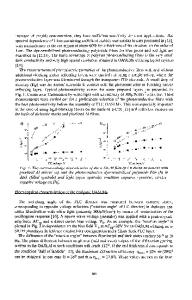
Preliminary Results on Large Area X-Ray a-SiC:H Multilayer Detectors with Optically Addressed Readout Manuela Vieira1, Yuri Vygranenko1,2, Miguel Fernandes1, Paula Louro1, Pedro Sanguino1, Alessandro Fantoni1, and Reinhard Schwarz3 1 DEETC, ISEL, Rua Conselheiro Emidio Navarro, Lisbon, 1949-014, Portugal 2 Electrical and computer engineering, University of Waterloo, Waterloo, Ontario, N2L3G1, Canada 3 Fisica, IST, Lisbon, 1049-001, Portugal ABSTRACT This paper investigates the feasibility of using a large area image sensor with an optically addressed readout for medical X-ray diagnostic imaging. The device prototype comprises a multilayer glass/ZnO:Al/p (a-SiC:H)/i (a-Si:H)/ n (a-SiC:H)/ i(a-Si:H)/p (a-SiC:H)/ a-SiNx/ITO structure coupled to a scintillator layer. Here, the p-i-n-i-p structure works in both sensing and switching modes depending on the biasing conditions. A numerical simulation is used to optimize the semiconductor layer thicknesses in order to achieve a photocurrent matching between back-to-back diodes in switching mode. The charge carrier transport within the p-i-n-i-p structure is also analyzed under different electric and optical biasing conditions. A physical model supports the results. INTRODUCTION Flat-panel digital radiography systems have recently been introduced as a new digital radiography technology [1, 2]. Modern hydrogenated amorphous silicon (a-Si:H) based radiographic imagers have active areas up to 17x17 sq. inch with the pixel pitch ranging from 127 to160 µm [3]. 3D pixel architecture was developed to integrate a switch use TFT with photodiode coupled to scintillator [4]. Specially designed charge amplifiers with extreme performances are used to attain a system noise in the range 1000-2000 electrons. The complexity of the array and associated electronics make these devices very costly. While these systems meet the requirements of the technology in terms of size and imaging performance, numerous innovations can be expected to increase the sensitivity and resolution, improve the device yield, as well as to reduce device cost. Typical pixel architecture consists of an a-Si:H n-i-p sensing diode and a TFT switch. The signal charge is stored on the sensor capacitance during the integration period, and is subsequently transferred to an external charge-sensitive amplifier during readout phase via the TFT switch. An alternative pixel design consists on the integration of the sensing element with an optoelectronic switch in order to enable an optically addressed readout. This paper reports on design, fabrication, characterization and modeling of an X-ray image sensor with an optically addressed readout. The implemented concept is the conversion of the X-ray image into an optical image by a scintillator and the conversion of the optical image into an electric one by a large area Laser Scanned Photodiode (LSP). We discuss the device operating principles, along with device characterization and numerical simulation results.
EXPERIMENT Figure 1 shows a schematic diagram of an X-ray
Data Loading...