Preparation of GaAs SOI and its Laser Recrystallization
- PDF / 1,862,443 Bytes
- 6 Pages / 417.6 x 639 pts Page_size
- 96 Downloads / 335 Views
PREPARATION OF GaAs SOT AND ITS LASER RECRYSTALLIZATION
LI XIQIANG, CHEN ZHIHAO, LIN CIIENGLU AND WANG WEIYUAN Shanghai Institute of Metallurgy, Academia Sinica, Shanghai,
China
ABSTRACT GaAs SO1 consisting of a sputtered GaAs film on a Si02 --Si or sapphire substrate is irradiated by CW Ar+ laser beam with a view to investigating its recrystallization. Using AES, x--ray diffraction, TEM and ED, we have studied the compositions, crystal orientations and grain size of the laser--irradiated GaAs films. The possible application of GaAs SO1 to devices is discussed on the basis of the experimental results.
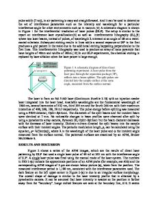
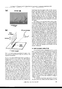
INTRODUCTION A considerable amount of work has been carried out recently on the beam crystallization of Si semiconductor on insulator (Si SO1) in an attempt to prepare Si three-dimensional integrated circuits [1], which is also one of the interesting topics in this conference. Although some preliminary results have been published in the literature for GaAs, such as the fabrication of GaAs SO1 [2], the laser recrystallization of GaAs material [3,4], the activation of implanted ions in GaAs [5], the formation of H-GaAs ohmic contacts [6], and the annealing of GaAs SOM [7] (semiconductor on metal), we have not seen any report on the CW Ar+ laser recrystallization of GaAs SO1 and its device fabrication. In this paper, preparation of GaAs SO1 films and their laser recrystallization have been investigated. Using AES, x-ray diffraction, TElland ED we have studied the compositions, crystal orientations and grain size of the laser-irradiated GaAs films. The possible application of GaAs SO1 to devices is discussed on the basis of the experimental results. EXPERIMENTAL The GaAs films are deposited using conventional RF sputtering equipment with a source power of 3 KW at a frequency of 13.5 MC. Undoped or Te-doped 8 3 GaAs crystals with a carrier concentration of -101 cm- are used as the target which is grounded by the shield at its edges [8]. There is a heater at the back of the substrate holder, and the substrate temperature can be measured by means of a Ni'Cr thermocouple. There are two kinds of substrates, thermally oxidized Si with ~6000 R Si02 on it (Si0 2 .- Si), and (1102) sapphire. The sputtering system can be pre-evacuated to a pressure of 10- 6 torr. The target and substrate are presputtered to etch their surfaces, then the deposition proceeds under a pure Ar atmosphere with a pressure of 0 1-2xlO- torr and substrate temperature of 280-340 C. For the samples used for laser irradiation, a CVD Si0 2 layer on the GaAs SO1 is used as an encapsulation film. The power of the CW Ar+ laser used for recrystallization of GaAs SO1 is 2.5-8 W and the circular beam is 60-80 pm in diameter. The power stability during laser processing is superior to 5% and the temperature of the sample 0 holder can be raised to 300-500 C as needed. The sample moves at 2 cm/s in scanning direction with 20-30 pm steps between lines. The protecting SiO2 should be carefully removed from laser-irradiated
Mat. Res. Soc. Symp.Proc. Vol. 23 (1984) @Else
Data Loading...