Probing the Nucleation of a Thin Metal Film: Atom Deposition Vs. Cluster Beam Deposition
- PDF / 1,640,232 Bytes
- 6 Pages / 414.72 x 648 pts Page_size
- 17 Downloads / 374 Views
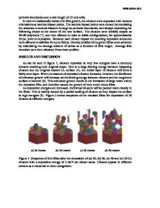
ABSTRACT The structure, morphology and epitaxy of nanometer scale solid clusters of gold atoms supported on the atomically flat basal (0001) plane of MoS 2 are studied by TEM and STM. These metal film nuclei are deposited onto the substrate, which is held at 4000C, by two different methods: (1) vacuum evaporation (PVD) and (2) soft landing of preformed Au clusters (CBD). In both cases the nuclei are single fcc crystals. In the case of atomic deposition the nuclei assume the shape of truncated tetrahedra with all their facets Au (111) planes. In the case of soft landed clusters the nuclei retain their free space morphology, that of truncated octahedra with hexagonal Au (111) and square Au (100) faces. Both PVD and CBD nuclei are heteroepitaxially aligned with (111)Au 11(0001)MoS 2 ; [220]Au II[11201MoS 2. INTRODUCTION The study of nanometer-size metal clusters on atomically flat substrates is of interest in regard to understanding the cluster/support interactions in heterogeneous catalysts and to understanding the processes underlying the nucleation and growth of ultra-thin metal films. The growth of a PVD metal film is pictured as occurring in three steps: first, adsorbed atoms condense at specific surface sites to form small solid nuclei; next, these nuclei grow by incorporation of additional adsorbed atoms and mobile metal clusters; finally, the density of clusters on the surface saturates and as the film continues to develop these metal islands coalesce [1]. The relative magnitudes of the interactions between the metal atoms themselves and between the metal atoms and substrate largely determines whether the nuclei grow as planar or three dimensional crystals. This in turn has important consequences with respect to the microstructure of the resulting thin metal film. We have been interested for several years now in the behavior of preformed clusters when they are soft landed onto solid supports [2-6]. It has been proposed that soft landing of preformed clusters may be a way to fabricate an ideal electrical interface between the resulting metal film and certain compound semiconductors and high T, superconductors [7]. In an attempt to better understand the differences between cluster beam deposition (CBD) and conventional atomic deposition (PVD) we compare in the present paper the atomic structure and morphology of nanometer-size Au nuclei deposited on (0001) MoS 2 by each of these processes. EXPERIMENTAL Substrate Preparation The MoS 2 substrates were thin flakes cleaved from a natural crystal of MoS 2 (Ward's Natural Science Establishment). They were prepared by first exposing a fresh surface on 83 Mat. Res. Soc. Symp. Proc. Vol. 355 0 1 99 5 Materials Research Society
L
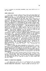
Oven Gas Quench
Gas
Furnace
u
MoS
Au o
2
Cleavage Flake
Aun
0
0 -0 Heating
Quench Gas
Pump
Zone
Pump
Oven Gas
TEN1 e 1
STM 0-lO2
I e -
Figure 1: Schematic of the cluster beam source and MoS 2 substrate. the crystal by cleaving with cellophane tape. Thin flakes were then peeled from the crystal using tweezers and glued onto 4
Data Loading...