Process-Structure Relationships of Nitrided Oxides and Oxynitrides
- PDF / 91,013 Bytes
- 6 Pages / 612 x 792 pts (letter) Page_size
- 70 Downloads / 307 Views
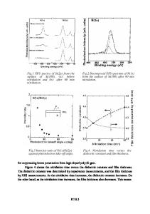
Process-Structure Relationships of Nitrided Oxides and Oxynitrides Anindya Dasgupta and Christos G. Takoudis Advanced Materials Research Laboratory, Department of Chemical Engineering University of Illinois at Chicago, Chicago, IL 60607, U.S.A. ABSTRACT The presence of nitrogen in the dielectric films is known to impart highly desirable properties in the ultra-large-scale-integration era; the position, amount and concentration profiles of nitrogen are therefore of great interest. In this work, we investigate two-step processes leading to bimodal nitrogen profiles, with one nitrogen peak near the Si/dielectric interface and the other near the dielectric surface. At 1000 oC and 1 atm, a nitridation step with NH3 following either an oxidation (in O2) or oxynitridation (in N2O) step is found to result in a bimodal nitrogen concentration profile for short nitridation times. Increasing the duration of the nitridation step with NH3 is found to completely nitridate the entire film. Secondary Ion Mass, Angle Resolved X-Ray Photoelectron, and Fourier Transform Infrared Spectroscopic studies are shown to support these observations. Therefore, based on such process-property-structure relationships, the engineering of desired nitrogen concentration profiles in nano-dielectric materials of interest becomes possible. Such knowledge may have significant implications on micro- and nano-electronic applications of silicon oxynitrides. INTRODUCTION Silicon oxynitrides have been the focus of attention for over a decade in ultra-large-scaleintegration (ULSI), since the incorporation of N in the dielectric film yields an increased dielectric constant compared to that of silicon oxides [1-10]. Moreover, oxynitrides provide enhanced thickness control, due to their self-limiting growth, and they are reported to improve the performance as a diffusion barrier of boron from the p+-gate layer during subsequent high temperature processing steps [1]. Further, since N imparts properties like improved hot-carrier resistance, reduced interface state generation, and longer device life time, it is imperative to have N at the substrate/dielectric interface and near the dielectric surface. Therefore, within such dielectric layers, it would be very useful to have desired N concentration profiles engineered for the optimal performance of any application of interest. Silicon oxynitrides can be grown using ammonia (NH3), nitrous oxide (N2O) and nitric oxide (NO) ambient [1-10]. Since oxynitrides grown in N2O or NO show a relatively small increase in the dielectric constant of the film, NH3, which is known to incorporate increased amounts of N, can be used as an alternative precursor. Thermal growth in N2O [1,4,6] has been generally seen to incorporate N near the oxynitride/substrate interface, while post annealing such an oxynitride layer in NH3 could start incorporating nitrogen near the dielectric surface. This might thus provide a bimodal N concentration profile within the dielectric. When the duration of annealing in NH3 is increased, nitridation of the
Data Loading...