Raman spectroscopy of nanograins, nanosheets and nanorods of copper oxides obtained by anodization technique
- PDF / 1,564,621 Bytes
- 7 Pages / 432 x 648 pts Page_size
- 4 Downloads / 286 Views
MRS Advances © 2019 Materials Research Society DOI: 10.1557/adv.2019.413
Raman spectroscopy of nanograins, nanosheets and nanorods of copper oxides obtained by anodization technique. M. Díaz-Solís, A. Báez-Rodríguez, J. Hernández-Torres, L. García-González, L. ZamoraPeredo* Centro de Investigación en Micro y Nanotecnología, Universidad Veracruzana, Adolfo Ruiz Cortines 455, C.P. 94294, Boca del Río, México.
*email: [email protected].
Abstract
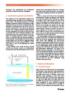
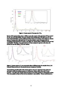
Different nanostructures such as: CuOH nanorods, CuO nanosheets and Cu2O nanograins were obtained by anodization approach at room temperature during times from 10 to 40 minutes. By scanning electron microscopy technique, it was found that Cu 2O nanograins were formed at 10 minutes, CuO nanosheets vertically oriented on nanograins were observed at 20 and 30 minutes, and from 20 minutes CuOH nanorods with low vertical orientation on nanosheets were formed, coexisting the three types of nanostructures at the same system. In samples without thermal treatment were observed that Raman spectra of nanograins have a typical signal at 218 cm-1 associated to Cu2O, Raman spectra of nanosheets have signals at 287 and 630 cm-1 associated to CuO and Raman spectra of nanorods, it was observed that Raman spectrum is dominated by an intense signal associated to CuOH located around 488cm-1. In addition, after 3 hours of thermal treatment at 300 °C, the morphology was conserved, and the hydrogen-related compound decreased. Raman spectra of nanorods only presented a signal at 287 cm-1 associated to CuO whereas in nanosheets three peaks at 150, 218, 304 cm-1 associated to the Cu2O were observed.
INTRODUCTION Nanostructured metal oxide semiconductors had been the subject of many scientific researchers for the last decades because of their exceptional properties and remarkable applications in biomedicine, photocatalysis, optoelectronic, energy industry,
Downloaded from https://www.cambridge.org/core. Columbia University - Law Library, on 06 Dec 2019 at 01:49:03, subject to the Cambridge Core terms of use, available at https://www.cambridge.org/core/terms. https://doi.org/10.1557/adv.2019.413
among others [1-5]. A candidate material for these applications that continues being the target of researchers is copper oxide due to has been considered as one of the most important metal oxide semiconductors because of its unique properties such as photocatalytic and photovoltaic properties, large surface area, potential quantum size effect and the bandgap range of main phases CuO and Cu 2O which are in a range of 1.7 to 2.2 eV [6-8]. Due to these properties it is imperative to comprehend their lattice dynamics, which have been studied experimentally in many research papers by Raman spectroscopy, infrared (IR), etcetera [9]. Nevertheless, the amount of morphologies that nanostructured copper oxides can adopt is extensive therefore the discussion to understand the electronic and vibrational properties of this material is still a challenge for researchers [10]. On the other hand, the massive production of
Data Loading...