Raman Spectroscopy of Si Nanocrystals in Nanocrystalline Si Superlattices: Size, Shape and Crystallographic Orientation
- PDF / 494,882 Bytes
- 6 Pages / 612 x 792 pts (letter) Page_size
- 108 Downloads / 328 Views
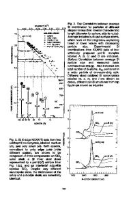
Raman Spectroscopy of Si Nanocrystals in Nanocrystalline Si Superlattices: Size, Shape and Crystallographic Orientation G. F. Grom*, P. M. Fauchet**, and L. Tsybeskov** * Materials Science Program, Department of Mechanical Engineering ** Department of Electrical and Computer Engineering University of Rochester, Rochester, NY 14627, U.S.A. J. P. McCaffrey, H. J. Labbé, and D. J. Lockwood Institute for Microstructural Sciences, National Research Council, Ottawa K1A OR6, Canada B. E. White Digital DNA Laboratories, Motorola, Austin, TX 78721, U.S.A. ABSTRACT We use Raman spectroscopy to study the size, shape and crystallographic orientation of silicon nanocrystals formed by solid phase crystallization of amorphous Si/SiO2 superlattices (SLs) grown by radio-frequency sputtering. The first and second Raman peaks broadening, their relative positions and intensities indicate the presence of nanoscale Si objects with a degree of disorder (grain boundaries) and strain (Si/SiO2 interfaces). Shapes of Si nanocrystals sandwiched between SiO2 layers strongly influence the Si/SiO2 interface roughness, which is inferred from the intensities of folded acoustic phonon scattering. The averaged crystallographic orientation of Si nanocrystals is determined by polarized Raman analysis. The laterally elongated nanocrystals exhibit preferred crystallographic orientation along the SL axis due to orientationdependent crystallization rates. These results demonstrate that control over Si nanocrystals structural parameters has been achieved and that solid phase crystallization of nanometer-thick amorphous Si films remains one of the most promising techniques for Si-based nanoelectronic device fabrication. INTRODUCTION Fabrication and characterization of nanoscale Si structures are of great technological importance due to their potential applications in nanoelectronic devices. Precise control over structural parameters (e. g. size, shape, and crystallographic orientation) of Si nanostructures and their microelectronics processing compatibility are required for reliable modeling and fabrication of nanoscale Si-based devices. Several years ago, we began to study silicon nanocrystals that are formed upon solid phase crystallization of amorphous Si/SiO2 superlattices (SLs) grown by radio-frequency (rf) sputtering [1]. We demonstrated that the vertical size of Si nanocrystals is equal to the thickness of initially deposited a-Si layers. We confirmed an excellent periodicity in nanocrystalline (nc)-Si/ amorphous (a)-SiO2 SLs, and proved presence of planar and chemically abrupt nc-Si/a-SiO2 interfaces. In this paper we present results of a comprehensive study of structural parameters of Si nanocrystals using Raman spectroscopy and complementary TEM analysis. In particular, crystallinity of the material, sizes of Si nanocrystals and presence of mechanical strains are F6.1.1
examined using first and second order Raman scattering. Raman spectroscopy of the folded acoustic phonons is employed to investigate the shapes of Si nanocrystals. The averaged cr
Data Loading...


