Relation between Leakage Current in PIN Photodiodes and Defects in InGaAs(P)/InP Heterostructures Grown Low Pressure MOC
- PDF / 2,274,044 Bytes
- 6 Pages / 420.48 x 639 pts Page_size
- 16 Downloads / 316 Views
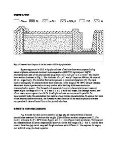
RELATION BETWEEN LEAKAGE CURRENT IN PIN PHOTODIODES AND DEFECTS IN InGaAs(P)/InP HETEROSTRUCTURES GROWN BY LOW PRESSURE MOCVD D.G. KNIGHT, C.J. MINER AND AJ. SPRINGTHORPE Bell-Northern Research, P.O. Box 3511 Sin C, Ottawa, Ontario, Canada KIY 4H7 ABSTRACT High resolution maps of the InGaAs photoluminescence intensity over whole 50mm diameter PIN detector wafers grown by low pressure MOCVD were obtained using a scanning photoluminescence (PL) system. The leakage current of PIN detectors was found to decrease exponentially with increased PL intensity. This correlation was quantitatively valid for both variation on a given wafer and for wafer-to-wafer variations. The density of morphological features on the surface of InGaAs(P)/InP heterostructures also was found to decrease exponentially with increased PL intensity, where a simple linear relationship between leakage current and feature density was then determined. The features are likely a manifestation of substrate defects which propagate from the surface of poor quality substrates. INTRODUCTION Low capacitance and dark current are necessary for the use of PIN photodiodes as low noise large-bandwidth detectors in fiber optics communication systems. The low pressure MOCVD technique has provided an excellent source of material for these detectors, where leakage currents as low as 3pA @ -10V and 1001gm device diameter have been achieved over a large substrate area[l]. The device structure used to achieve this is shown in Figure 1. The diode has a planar structure, with a p+-n junction formed in the InGaAs layer by diffusing Zn through the InP cap layer. However, fabrication of devices using substrates from many different boules of InP from different suppliers has caused Cr/Au SiNX us to realize that the quality of the substrate material critically affects the n-Inp p+ -Si02 leakage currents of the PIN detectors made. Qualifying substrates by aAs r-ln~ time a is processing entire wafers consuming and expensive task, so a n-InP technique which would determine the quality of the material before processing n.- In P Recently, would be highly desirable. Haussler et al.[2] have shown that the room temperature photoluminescence Cr/Au (PL) intensity of the InGaAs layer in a detector structure is correlated with the leakage current of the processed devices. These authors were determining the Fig. 1 Schematic cross section of a effect of substrate ion implantation on planar InGaAs/InP PIN photodiode. the InGaAs PL intensity directly after crystal growth. In this work, a detailed study of the relationship between the room temperature PL and leakage current of PIN detectors will be conducted. This will determine the effect of substrate quality on device performance, as opposed to the effects of different processing steps studied by Haussler et al. It will be shown that the PL intensity also correlates with the number density of morphological defects that appear on the surface of InGaAsP epilayers. The probable role of these features as the cause of leakage current in PIN diodes wi
Data Loading...


