Reliable Local Strain Characterization on Si/SiGe Structures in Biaxial Tension
- PDF / 3,207,475 Bytes
- 7 Pages / 612 x 792 pts (letter) Page_size
- 65 Downloads / 261 Views
0958-L04-08
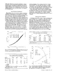
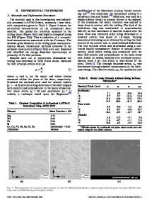
Reliable Local Strain Characterization on Si/SiGe Structures in Biaxial Tension Wenjun Zhao1, Gerd Duscher2,3, Mohammed A. Zikry4, and George Rozgonyi5 1 Materials Science and Engineering, North Carolina State University, 911 Parnters Way, RM 3074 EB1, RALEIGH, NC, 27606 2 MSE, North Carolina State University, 911 Parnters Way, RM 3074 EB1, RALEIGH, NC, 27606 3 Oak Ridge National Lab, Oak Ridge, TN, 37831 4 Mechanical and Aerospace Department, North Carolina State University, RALEIGH, NC, 27606 5 Materials Science and Engineering, North Carolina State University, RALEIGH, NC, 27606 Abstract The strain in the strained Si layer on a blanket strained Si/SiGe structure could not be determined with only convergent beam electron diffraction due to high order Laue zone (HOLZ) line splitting. Combined with CBED and finite element calculations, we quantified the deformation field by measuring HOLZ line splitting and demonstrated a procedure to determine the initial strain in the strained Si layer. Our results also gave us insights in strain relaxation in a TEM sample. The CBED technique combined with FE modeling has the potential for strain measurements on new generation strain-enhanced structures. With the gate length shrinking down to sub-100nm, direct experimental strain measurement becomes more challenging since the area of most interest is only tens of nanometers wide and a few nanometers down below the gate. Among all of the strain measurement techniques, convergent beam electron diffraction (CBED) is the only method that can offer a spatial resolution on a nanometer scale1,2. However strain relaxation always happens in a TEM Sample. Clement et al.3 examined a NiSi layer in a n-MOS transistor and showed the broadening of HOLZ lines is mainly due to the atomic plane bending that occurs as a result of the stress relaxation during the TEM sample preparation. For CMOS transistor with uniaxial strain in the channel, clean CBED pattern can be obtained near the center of the channel therefore strain retained in the TEM sample can be determined4,5. While for structures with biaxial strain, little work has been reported. In this paper for the first time we present our strain measurements on strained Si/SiGe structure with biaxial strain. The CBED experiments were taken on a JEOL 2010F scanning transmission electron microscope equipped with a Gatan GIF 200 energy filter, scanning unit (STEM mode) and a slow scan rate 1024×1024 CCD camera. The microscope was operated on 200keV. An energyselecting slit with a width of 10eV was inserted and centered around the zero-loss peak so that inelastic scattered electrons can be filtered out. The sample investigated was a blanket structure of a 20nm Si on SiGe substrate. The thickness was determined to be around 300nm with (400) fringes under two beam conditions. Figure 1 (a) show the structure of the blanket strained Si/SiGe heterostructure with a 20nm thin strained Si layer and a thick constant SiGe buffer with 20% Ge. The CBED measurements were performed deep in the constant
Data Loading...