Requirements on Organic Electro-Optic Devices for Aerospace Applications
- PDF / 50,657 Bytes
- 7 Pages / 432 x 648 pts Page_size
- 72 Downloads / 308 Views
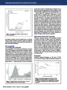
require fiber because of weight considerations (vis à vis coax or waveguide), low loss, broad bandwidths, phase stability or EMI mitigation. Electro-optic polymer photonic devices are particularly attractive for very high frequency and broadband applications since the basic electro-optic interaction involves an intra molecular electronic transition. Even mm-waves are essentially “low frequency” compared to the fundamental chromophore resonance in the visible portion of the spectrum. Electro-optic device performance has been demonstrated up to 113 GHz 1. This high frequency and broadband capability is of particular interest given the 17.8-21.2 GHz and 25.25-31.3 GHz mobile, broadcast and fixed satellite services bands and the 37.0 GHz and higher all satellite services including ISL bands. Polymer devices are implemented with thin film technology that has the capability of hybridization onto Si, GaAs, ceramic or flexible2 substrates. For space applications, they are expected to exhibit minimal ionizing radiation damage cross section since they mainly consist of thin layers of the light elements H, C, N and O. Finally, there is a significant development potential for devices with RF gain, low noise figure, low power operation and signal processing functions such as frequency conversion and efficient harmonic generation. POLYMER PHOTONICS The “customer” for polymer photonic components is ultimately a system supplier who is only concerned about performance and cost. The performance issues that the system supplier may be concerned with at the subsystem level for the RF portions of the system are parameters such as gain (G), noise figure (NF), intermodulation products (IP2 and IP3), cross talk, electromagnetic interference (EMI), etc. At the material end of the “food chain” shown in Figure 1 are such material properties as refractive index (n), dielectric constant (εr), density, spectral absorptance (α) and, for non-linear optical (NLO) active electro-optic materials, the molecular properties of hyperpolarizability (β) and dipole moment (µ). As we work our way up the food chain, the material processing associated with orienting the molecular dipole moments results in a bulk material property described by the electro-optic coefficient (rm n) which is a function of β, the number density of NLO molecules (N) and their effective orientation (). The orienting process (“poling”) may also change α of the bulk material (by a little understood Gain (G) Noise Figure (NF)
RF Subsystem Parameters G∝1/Vš 2 NF∝Vš 2 Half-Wave Photonic Component Voltage (Vš) Parameter λh Vš = n3r33L Electro-Optic Bulk Material Coefficient (r33) Parameter r33=Nβ Hyperpolarizabilityβ)( Dipole Moment (µ)
Microscopic Molecular Parameters
Figure 1. The language of Figures-of-Merit
phenomenon called “poling induced loss”). The device engineer will then utilize the NLO material in the fabrication of a modulator such as the Mach-Zehnder modulator3 (MZM ) whose performance may be characterized by its sensitivity (Vπ), insertion loss (ηopt), and bandwidth (B
Data Loading...