Sb 2 Te 3 and Bi 2 Te 3 Thin Films Grown by Molecular Beam Epitaxy at Room Temperature
- PDF / 2,873,684 Bytes
- 6 Pages / 612 x 792 pts (letter) Page_size
- 117 Downloads / 422 Views
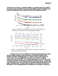
Sb2Te3 and Bi2Te3 Thin Films Grown by Molecular Beam Epitaxy at Room Temperature Z. Aabdin1, M. Winkler3, D. Bessas2, J. König3, N. Peranio1, O. Eibl1, R. Hermann2, and H. Böttner3 1 Institut für Angewandte Physik, Universität Tübingen, Auf der Morgenstelle 10, D-72076 Tübingen, Germany 2 Institut für Festkörperforschung, Forschungszentrum Jülich GmbH, Leo Brandt Strasse 1, D-52425 Jülich, Germany 3 Fraunhofer Institut Physikalische Messtechnik, Heidenhofstrasse 8, D-79110 Freiburg, Germany ABSTRACT Nano-alloyed p-type Sb2Te3 and n-type Bi2Te3 thin films were grown on SiO2/Si and BaF2 substrates by molecular beam epitaxy (MBE) in two steps: (i) Repeated deposition of fivelayer stacks with sequence Te-X-Te-X-Te (X = Sb or Bi) with elemental layer thicknesses of 0.2 nm on substrates at room temperature, (ii) annealing at 250 °C for two hours at which phase formation of Sb2Te3 or Bi2Te3 occurred. The room temperature MBE deposition method reduces surface roughness, allows the use of non lattice-matched substrates, and yields a more accurate and easier control of the Te content compared to Bi2Te3 thin films, which were epitaxially grown on BaF2 substrates at 290 °C. X-ray diffraction revealed that the thin films were single phase, poly-crystalline, and textured. The films showed grain sizes of 500 nm for Sb2Te3 and 250 nm for Bi2Te3, analyzed by transmission electron microscopy (TEM). The in-plane transport properties (thermopower S, electrical conductivity σ, charge carrier density n, charge carrier mobility μ, power factor S2σ) were measured at room temperature. The nano-alloyed Sb2Te3 thin film revealed a remarkably high power factor of 29 μW cm-1 K-2 similar to epitaxially grown Bi2Te3 thin films and Sb2Te3 single crystalline bulk materials. This large power factor can be attributed to a high charge carrier mobility of 402 cm2 V-1 s-1 similar to high-ZT Bi2Te3/Sb2Te3 superlattices. However, for the nano-alloyed Bi2Te3 thin film a low power factor of 8 μW cm-1 K-2 and a low charge carrier mobility of 80 cm2 V-1 s-1 were found. Detailed microstructure and phase analyses were carried out by energy-filtered TEM in cross-sections. Quantitative chemical analysis by energy-dispersive x-ray spectroscopy (EDS) was also applied. In Bi2Te3 thin films, few nanometer thick Bi-rich blocking layers at grain boundaries and Te fluctuations by 1.3 at.% within the grains were observed. The small charge carrier densities are explained by a reduced antisite defect density due to the low temperatures to which the thin films were exposed during annealing. INTRODUCTION Peltier materials based on Bi2Te3, are widely used for room temperature applications due to their high thermoelectric figure of merit ZT = (S2 σ / λ) T ≈ 1 at T = 300 K. Increase of ZT beyond 1 in bulk materials is difficult to achieve since the transport properties depend on each other given by fundamental parameters of the electron and phonon system. Hicks and Dresselhaus predicted a ZT enhancement in low-dimensional system due to quantum confinement and lattice phonon sca
Data Loading...