Segregant-Assisted Growth of SiGe/Si Heterostructures and their Optical Properties
- PDF / 574,908 Bytes
- 10 Pages / 414.72 x 648 pts Page_size
- 8 Downloads / 288 Views
This is
because they have not only a high potential to improve Si-based electronic devices such as bipolar transistors and p-channel MOSFETs by introducing
heterointerfaces but also a possibility to realize light emitting devices by exploiting their high luminescence efficiency. It is therefore natural that there is a strong demand for realization of high quality strained SiGe/Si quantum wells (QWs) and superlattices (SLs). Formation of abrupt heterointerfaces, however, is a critical issue in this system, since surface segregation of Ge atoms causes interfacial smearing during molecular beam epitaxial (MBE) growth which is frequently used for the growth of SiGe layers. Surface segregation is a reaction between impinging atoms and surface atoms of substrates. This phenomenon was firstly recognized to be important when MBE layers were doped with some kinds of impurities [1,21. It should be pointed out, however, that surface segregation generally takes place in cases of not only doping but also of heterointerface formation. Ge and In are now well known to segregate when forming Si-on-SiGe and GaAs-on-InGaAs heterostructures, respectively. To avoid segregation and obtain abrupt heterointerfaces, a low temperature growth has been thought to be essential. However, the low temperature growth sacrifices crystal quality and SiGe layers giving rise to band edge emission are not readily obtained. To improve crystal quality of MBE grown materials, several techniques were attempted including post-growth annealing. Interestingly, the annealing was found to result in the appearance of a broad emission peak which was not observed in SiGe alloy bulk crystals and band edge emissions were never observed [3]. Band edge emissions were confirmed in SiGe epitaxial films formed 191 Mat. Res. Soc. Symp. Proc. Vol. 318. 01994 Materials Research Society
by such gaseous growth methods as rapid thermal chemical vapor deposition [4]. However, we have recently shown that if we employ a high growth temperature, far
beyond the commonly accepted growth temperatures, highly luminescent SiGe/Si QWs providing band edge emissions can be formed [5].
The relationship between grow-
th conditions, especially growth temperatures, and luminescence efficiency of SiGe/Si heterostructures is discussed before the method to realize high quality SiGe/Si heterostructures with abrupt interfaces is introduced.
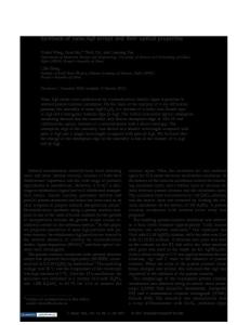
FORMATION OF LUMINESCENT SiGe/Si QWS BY SOLID SOURCE MBE Figure I shows growth temperature dependence of photoluminescence (PL) spectra of SiGe/Si QWs [5]. It is clearly seen that NP and TO peaks, which are attributed to no-phonon and transverse optic (TO) phonon assisted emissions originating from SiGe well layers, respectively, are well resolved in the case of growth at temperatures higher than 600 VU. On the other hand, no band edge emissions are observed in the samples grown at temperatures lower than 600 VU. Such growth temperatures higher than 600 VU have not been employed so far to avoid lattice relaxation and interface smearing. At higher temper
Data Loading...