Selective Deposition of Polycrystalline Silicon Thin Films by Hot-Wire CVD
- PDF / 2,058,976 Bytes
- 6 Pages / 414.72 x 648 pts Page_size
- 74 Downloads / 389 Views
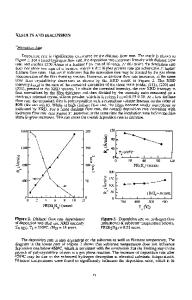
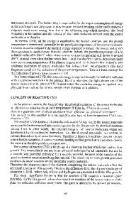
of microcrystalline silicon has been achieved by a pulsed gas [2] or a very high-frequency PECVD (VHF-PECVD) process [3] using SiH 4 and H2 as reactants, or a rf-plasma CVD process using SiF 4 and SiH 4 mixtures [4]. However, the deposition rates are low [2,3] and/or a substrate temperature higher than 300*C is required [4]. In this paper, we have demonstrated, for the first time, that selective deposition of polycrystalline silicon thin films can be achieved by hot-wire CVD at high deposition rate and low substrate temperature with excellent selectivity. Hot-wire CVD employs a heated tungsten filament to preactivate reactive gases. Its gas phase chemistry is simpler than that of PECVD, there are no film damages caused by bombardment of energetic species, and it is cost effective. A variety of good quality materials such as amorphous silicon and silicon nitride have been deposited at high growth rates by this method [5,6]. EXPERIMENT The hot-wire CVD system employed in this study has been described in detail in some previous papers [7,8]. In brief, we pass hydrogen gas over a tungsten filament heated at 18000 C. Molecular hydrogen is catalytically disassociated into atomic hydrogen. Unlike the hot-wire CVD process used by other groups [5,91, we let source gas disilane bypass the filament and react with atomic hydrogen down stream of the filament to form film forming species. In this way, we avoid both the generation of atomic Si which has a high sticking coefficient undesirable for good quality film and deterioration of the tungsten filament when silicon reacts with tungsten to form silicide. The deposition conditions used in this study are listed in Table I. The substrate temperature is monitored by a thermocouple clamped on the surface of the substrate holder close to the 411 0 Mat. Res. Soc. Symp. Proc. Vol. 403 1996 Materials Research Society
Table I. Deposition Conditions Filament temperature (Tf)
1800 °C 250 - 400 °C 40 - 100 mTorr 0.53 - 1.6 sccm 48 - 202 sccm
Substrate temperature (TO) Reactor pressure (Pd) Disilane flow rate Hydrogen flow rate
substrate. The filament temperature is monitored with a pyrometer through a quartz window on the reactor. The percentage of Si in the gas phase is varied by adjusting the flow rate of hydrogen or
disilane. The substrates used for selective deposition are obtained either by photolithography or by covering part of a SiO 2 substrate with a mechanical mask and sputtering Mo on to the exposed area. The film crystallinity and thickness are examined by cross-section transmission electron microscopy (TEM). The film crystallinity is also examined by high resolution TEM (HRTEM) and Raman spectroscopy. TEM samples are examined at 200 kV in a JEOL-2000FX transmission electron microscope. HRTEM samples are examined at 300 kV in a JEOL-4000EX transmission electron microscope. The Raman analysis is done on a Spex 1877 TRIPLEMATE spectrometer equipped with a Spex SpectrumOne liquid nitrogen cooled CCD detector system. The 488-nm line of an Ar+ laser is used as the excitation s
Data Loading...