Sharp absorption and high temperature thermal emission from simple metallic photonic crystals
- PDF / 349,529 Bytes
- 6 Pages / 612 x 792 pts (letter) Page_size
- 95 Downloads / 243 Views
1162-J02-05
Sharp absorption and high temperature thermal emission from simple metallic photonic crystals Rana Biswas1, Dayu Zhou2, Irina Puscasu3, Edward Johnson3, Andrew Taylor3, Weijun Zhao2 Depts. of Physics & Astronomy, Ames Laboratory, Microelectronics Research Center, Electrical & Computer Engineering, Iowa State University, Ames, IA 50011 2 Dept. of Electrical & Computer Engineering, Microelectronics Research Center, Iowa State University, Ames IA 50011 3 ICX Photonics, Billerica, MA 01821 1
ABSTRACT We design and fabricate metallic photonic crystals with sharp absorption peaks in the infrared regime. We have fabricated a metallic photonic crystal consisting of a triangular lattice of holes in a silicon layer conformally coated with gold at a lattice pitch of 3.8 microns. Conventional lithographic and deep reactive ion etching was used. The photonic crystal exhibits a deep reflection minimum and sharp thermal emission peak near the lattice spacing. Measurements agree well with rigorous scattering matrix simulations. This simple single-layer structure with a single patterned exposure has no emission sidebands and can be scaled to other lattice spacings.
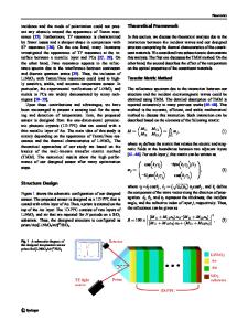
INTRODUCTION Metallic photonic crystals [1-3] and metallo-dielectric photonic crystals [4-5] have attracted much scientific interest in substantially modifying the thermal emission from the black body spectrum. These photonic crystals have a sharp absorption maximum at a wavelength controlled by the lattice spacing. When these crystals are heated, thermal emission is observed in a narrow wavelength band controlled by the absorption profile, and suppressed outside this band. Photonic-crystal based thermal emitters have diverse applications in the infrared regime as narrow band sources and sensors. At optical wavelengths, tailoring thermal emissivity is very important to improving efficiency of incandescent sources. Hence it is of much interest to design simple low-dimensional structures, that can be easily fabricated, where the width of the thermal emission can be controlled and made as narrow or broad, for wavelength-selective applications. The metallic woodpile structure has demonstrated a narrow thermal emission and band edge at a wavelength controlled by the period of the rods [1-3]. This structure has utilized several layers of stacked 1-dimensional pattern of metallic rods [1-3]. It is of interest to fabricate simple lowdimensional structures such as a single patterned metallic layer, that can demonstrate a sharp absorption feature and correspondingly sharp emission peak. In this paper we design and fabricate a very efficient absorber/emitter structure consisting of a triangular lattice of holes (radius R) and depth d1 with a period a in a metal film (Fig. 1). The hole radius R is small so that the wavelength cut-off for the fundamental TE(11) propagating mode in a circular waveguide (λc=3.42R) is less than a. No classical waveguide modes can transmit through the holes for incident wavelengths λ near a. The depth of the corrugated metal layer (d1) is t
Data Loading...