Si Implantation and Annealing of GaN for n-Type Layer Formation
- PDF / 1,716,973 Bytes
- 5 Pages / 414.72 x 648 pts Page_size
- 2 Downloads / 347 Views
conventional furnace annealing (FA) in N 2 or forming gas ambient. During anneal the GaN was placed either on a Si 3 N4 surface or on an another GaN wafer in close contact proximity [5].
RESULTS Since the implantation doping requires high temperature annealing, we have investigated the influence of different annealing conditions in the temperature range 700-1150"C on the surface
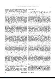
morphology and electrical properties of the as-grown GaN. The GaN thermal decomposition has been attributed to Ga liquid droplet formation [6,7]. We have correlated the effect of the Ga droplet formation on the electrical properties of the GaN. The surface of as-grown GaN used in this study is smooth. The morphology of the unprotected GaN surface did not change up to an RTA temperature of 1000"C. After 1050"C/15s anneal, few Ga liquid droplets were observed on the GaN surface as a consequence of N evaporation. As the time or the temperature of the anneals increased, the number of droplets also increased. The Ga liquid droplets formed after 1150"C/15s RTA are shown in Fig. l(a). The Ga droplets could be removed from the GaN surface by soaking the wafer in HCl. As shown in Fig. I(b) after HC1 soaking the SEM picture revealed holes in the locations where Ga droplets were previously present. The presence of the Ga droplets, however, did not change the integrated electrical properties as determined by the Hall measurements.
K
ii
I
(a)
(b)
Fig. 1. SEM micrographs of GaN surface. The samples were annealed at 1150°C/15s. (a) annealed surface, (b) HCI soaked after anneal. A further increase in the temperature or the time of the anneal, however, leads to coagulation of the Ga-rich liquid droplets. The appearance of Ga coagulation marks the end of the useful range of annealing. Under the coagulated areas the dissolution of the underlying GaN layer has been observed. The Ga droplet formation could be decreased only by suppressing the nitrogen evaporation. The close contact covering of the GaN surface with another GaN piece or with Si3N4 surface during the anneal, reduced the N evaporation. The surface morphologies of GaN heat-treated at 10000C for 30 min. with and without GaN proximity capping are shown in Fig. 2. As shown in Fig. 2(b) severe deterioration of the surface was observed in the area not covered by the GaN proximity cap. The surface morphology of the areas covered with the GaN proximity
184
cap is smooth, with only few Ga droplets. For the close contact covered areas the sheet resistivity and the mobility values are the same as those in the as-grown material.
(a)
(b)
Fig. 2. SEM micrographs of GaN surface annealed at 1000"C for 30 min. (a) Covered with GaN, (b) without GaN proximity capping. Our morphological study indicates that the GaN could be heat treated without Ga coagulation for an annealing temperature as high as 11 50"C using proximity capping if the anneal duration does not exceed 120s. Therefore, the Si activation RTA has been performed only up to this limit. First we present our implantation results on high resista
Data Loading...