Si Single-Electron SOI-MOSFETs: Interplay with Individual Dopants and Photons
- PDF / 618,511 Bytes
- 7 Pages / 612 x 792 pts (letter) Page_size
- 77 Downloads / 324 Views
1145-MM10-01
Si Single-Electron SOI-MOSFETs: Interplay with Individual Dopants and Photons Michiharu Tabe1, Zainal A. Burhanudin1,2, Ratno Nuryadi1, Daniel Moraru1, Maciej Ligowski1,3, Ryszard Jablonski3 and Takeshi Mizuno1 1
Research Institute of Electronics, Shizuoka University, 3-5-1 Johoku, Nakaku, Hamamatsu 4328011, Japan 2
Dept. of Electrical & Electronic Eng., University Technology Petronas, Malaysia
3
Division of Sensors and Measuring Systems, Warsaw University of Technology, A. Boboli 8, Warsaw 02-525, Poland
ABSTRACT We have demonstrated that Si single-electron or single-hole SOI-MOSFETs with the multi-dots channel have attractive new functions such as photon detection and single-electron transfer. Multi-dots formed by selective-oxidation-induced patterning of the thin SOI layer have been used in the experiments of photon detection, while, most recently, we have utilized smaller dots consisting of individual dopant potentials in single electron transfer devices. Furthermore, in order to directly observe spatial landscape of single charges in the channel region, we have developed Low Temperature-Kelvin Probe Force Microscopy and succeeded in detecting singledopant potential in the channel region. In this paper, photon detection by these devices will be primarily described.
INTRODUCTION Si single-electron-tunneling (SET) or single-hole-tunneling (SHT) devices have a great potential in realizing a variety of new functions. So far, we have fabricated multi-dots Si SET/SHT FETs by a couple of unique but simple methods, in which the channel region has a structure of mutually-connected patterned Si dots [1] or dopant-induced potential dots [2]. By using these devices with randomly-arranged multi-dots, we have obtained several important results of single-photon detection [1] and single-electron transfer [2]. Since in nanometer-scale devices we cannot avoid significant fluctuation of device structures and sizes, it is of great importance to create such useful photonic and electronic functions in the framework of fluctuation tolerant devices. In this paper, we will present our previous and most recent results primarily on singlephoton detection by multi-junction SHT devices as well as brief description of direct observation of individual dopant potentials of the channel regions in SOI-MOSFETs by Low TemperatureKelvin Probe Force Microscopy (LT-KFM) [3].
PHOTON DETECTION BY SHT Detection of photo-charges in SHT
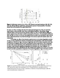
Single-photon detectors fabricated for quantum computing, medical imaging and other novel optoelectronic devices are primarily based on photomultiplier tube or semiconductor avalanche photodiodes. Recently, however, detectors based on SET transistors and other types of quantum devices are gaining more attention [4-6]. Those devices typically have an ensemble of dots with specific tunnel junction resistances and capacitances that will determine the SET current level. Under light illumination, absorbed photons can change the number of electrons in the dots, sensitively modulating the current level. Gen
Data Loading...