Si x C 1-x Electroluminescence Structures
- PDF / 235,052 Bytes
- 4 Pages / 420.48 x 639 pts Page_size
- 74 Downloads / 367 Views
Six C1 -x ELECTROLUMINESCENCE STRUCTURES C. FALCONY*, A. ORTIZ**, A. SANCHEZ** *Centro de Investigaciones y Estudios Avanzados del Fisica, Apdo. Postal 14-740, 07000, Mexico, D.F. **Instituto de Investigaciones en Materiales, UNAM., 360, Coyoac~n 04510, Mexico, D.F.
I.P.N., Apdo.
Depto. Postal
de 70-
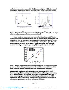
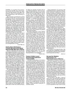
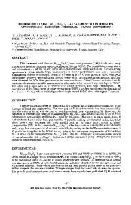
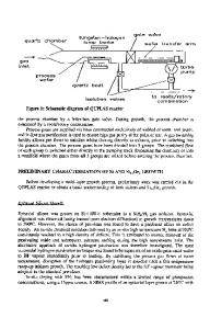
ABSTRACT The electroluminescent characteristics of multilayer structures involving Si C as the light emitting material are reported. The structures studieA have two types of multilayer stacks a) Si rich Si0 2 / Si0 2 1Si Cl v and b) Si rich SiO /Si C , , Both type of structures were deposite• on an n-type silicon surstrt-e and conductive indium oxide was deposited on top of the structure to define the electroluminescent device. The light emitted spectra present two broad peaks at %530 and 670nm when an undoped Si C layer is integrated in the structure. However, when a boron dopedX Sixt is used, the light emission at larger wavelengths is dominant. INTRODUCTION The quest for large area flat panel electroluminescent displays has spurred a considerable research activity on thin film based electroluminescent devices. In particular Si C •x thin film light emitting diodes have generated increasing interest from research groups working in this area [1,2]. Most of the devices reported are p-i-n type of structures. However, Kruangam et. al. [1] have reported recently a structure that involves a thin highly resistive layer of a-SiC. inserted between the p and i or the i and n layers of a p-i-n device. This layer acts as a tunneling barrier giving place to hot carrier injection across the structure. In the present work we report the electroluminescent characteristics of two types of silicon based structures [3,4] using Si Cl layer. These were a) Si-rich SiO 2 /SiO 2 /Six C1 and b) Si rich SiO 2 Si C . The Si C film was either undoped, Boron doped or a double layer otundoped and 6-doped Si C The luminescent spectra observed depend strongly on the type of sitic-n&xcarbide layer used. EXPERIMENTALS DETAILS AND RESULTS The deposition of the Si-rich SiO and SiO2 layers used in the fabrication of these devices has been described in detail in an earlier work (3,5). The technique used for this purpose was the atmospheric pressure chemical vapor (CVD) deposition technique using SiH4 and N2 0 as reactant gases and N2 as a carrier gas. A N 0 to SiH4 ratio (Ro) of 3 was used for the Si-rich Si0 2 and an Ro=200 for SiO2 . The deposition temperature was 700'C, and a postdeposition annealing treatment at IO00°C in flowing N2 was given to the Si rich SiO /SiO layers. Typical thicknesses were -2004 and -. 400A for the Si-ricg Si62, and SiO2 films respectively. The Si Clx films were deposited in an r.F coupled plasma-enhanced CVD system using SiH4 and CH4 as reactive gases. The substrate temperature during deposition was 250°C and the pressure was 600 mT. The total flux -of gases was 50 ccm. The p-doped Si C samples were prepared using B2H gas mixed with the reactive gasesxil--nthe desiredoamount. The thicknest of these films was in the range
Data Loading...