SiGe/Si Nanowire Axial Heterostructures Grown by LPCVD Using Ga-Au
- PDF / 1,866,250 Bytes
- 6 Pages / 612 x 792 pts (letter) Page_size
- 75 Downloads / 324 Views
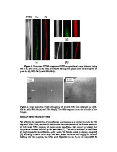
SiGe/Si Nanowire Axial Heterostructures Grown by LPCVD Using Ga-Au A. Rodríguez 1, T. Rodríguez 1, C. Ballesteros 2, J. Jiménez3 1 Tecnología Electrónica, Universidad Politécnica de Madrid, E.T.S.I.T., 28040 Madrid, Spain 2 Física, Universidad Carlos III, 28911 Leganés (Madrid), Spain 3 GdS Optronlab, Ed. I+D, Universidad de Valladolid, 47011 Valladolid, Spain ABSTRACT The use of Ga-Au alloys of different compositions as metal catalysts for the growth of abrupt SiGe/Si nanowire axial heterostructures has been investigated. The heterostructures grown in a continuous process by just switching the gas precursors, show uniform nanowire diameters, almost abrupt compositional changes and no defects between the different sections. These features represent significant improvements over the results obtained using pure Au. INTRODUCTION Axial SiGe-based nanowire (NW) heterostructures (HE) and superlattices are attractive for the design of advanced devices with potential applications in nanoelectronics; besides, their growth process may be compatible with current device fabrication technologies [1]. The most commonly used catalyst metal for the growth of semiconductor NWs by the Vapour-LiquidSolid (VLS) method is Au. This method combined with Chemical Vapour Deposition (CVD) techniques has been successfully used to grow Si and SiGe NWs of different compositions. In principle, axial SiGe/Si NW HEs are easy to produce using this process by just switching the gas precursors. However, an important feature of the Au-Si and Au-Ge binary phase diagrams is the high atomic concentration of Si or Ge in the liquid at the usual growth temperatures [2]. If a SiGe/Si HE is being grown and the composition of the precursor gas is changed, the Ge still dissolved in the metal has to be diluted out of the droplet to get a pure Si nanowire segment. Considering that several full droplet fillings are required to get the dissolved Ge out of the droplet, the result will be a compositionally graded junction. It has been shown that this is indeed the case, and also that the length of the transition region scales with the nanowire diameter [3]. The VLS growth of Si NWs using other metals, like Ga or In has been considered [4, 5]. These metals show very low solubilities of Si and Ge, an effect that could be advantageous to improve the abruptness of interfaces in Ge/Si and SiGe/Si NW HEs [2]. However, they are not catalytic, so conventional CVD cannot be used and plasma assisted CVD techniques are required [4-6]. The use of alloys of catalytic and non-catalytic metals, like Ga-Au, appears as an alternative to take advantage of the properties of both species using a conventional CVD process. Ga-Au alloys have been used already for the growth of high quality Si NWs by CVD [7]. Cylindrical and straight SiGe NWs of good crystalline quality and an almost constant composition have also been grown by Low Pressure CVD (LPCVD) using Ga-Au alloys [8]. In this last case, it has also been shown that the interfaces between the NW and the metal droplet are sharper than
Data Loading...