Silicide Mediated Grown Silicon Thin Films for Photodiodes
- PDF / 3,598,534 Bytes
- 6 Pages / 595 x 842 pts (A4) Page_size
- 22 Downloads / 338 Views
0974-CC01-12
Silicide Mediated Grown Silicon Thin Films for Photodiodes Joondong Kim1,2, Wayne A. Anderson1, Chang-Soo Han2, and Eung-Sug Lee2 1
Electrical Engineering, University at Buffalo, State University of New York, Bonner Hall, Buffalo, NY, 14260 2
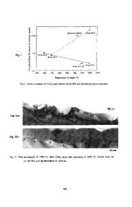
Nano-Mechanical Systems, Korea Institute of Machinery and Materials, 171 Jang-dong, Yuseong, Daejeon, 304343, Korea, Republic of ABSTRACT Quality Si thin films were grown by the metal-induced growth (MIG) method. Metal (Co, Ni, or mixing of Co and Ni) was thermally evaporated on a 200 nm-SiO2 coated Si wafer. Si sputtering was performed at 600 – 620 oC in a dc magnetron system. The reaction of Si and metal first formed a silicide (CoSi2 or NiSi2) layer and further Si sputtering grew a Si film above it. The grown Si films were practically fabricated for Schottky photodiodes and electrically measured under one sun scan illumination (100 mW/cm2). The mixing of Co and Ni case improved the short circuit current density of 10.6 mA/cm2, which is one order higher than that for the single Co catalyst case. INTRODUCTION Low temperature Si crystallization has been intensively researched for use in thin film transistors (TFT) [1,2], solar cells, flat panel displays [3] and image sensors [4]. It has been found that addition of metal catalysts such as Ag, Au, Al, Pd, Ni and Co greatly relaxed the need for high processing temperature. This advantage of metalinduced crystallization (MIC) facilitates Si crystallization for various applications. Metal-induced lateral crystallization (MILC) has evolved to manipulate selective crystallization and reduce metal contamination in TFT applications [3]. The metalinduced growth (MIG) method is a dynamic reaction of metal and Si resulting in direct formation of a polycrystalline Si (poly-Si) thin film without an additional crystallization step. This study is also a good comparison to MIG silicide nanowire growth and nanoscale contact schemes [5,6].
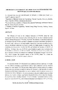
EXPERIMENTAL DETAILS A SiO2 layer of 200 nm thickness was first deposited on the substrate by plasma enhanced chemical vapor deposition acting as a buffer layer against metal diffusion into the Si substrate. Various metal catalyst layers were formed by Co 30 nm, Ni 30 nm, or Co coated Ni (Co 10 nm/Ni 10 nm/Co 10 nm). Si was sputtered from a Si target by dc magnetron. The sputtering process was performed in 5 % H2/Ar, where Ar was used as a carrier and H2 passivated dangling bonds. The metal catalyst first reacted to sputtered Si forming a silicide layer, which roles as a template to grow a poly-Si thin film by further Si sputtering with a little lattice misfit. For poly-Si film growth, higher power Si sputtering (2.12 – 8.5 W/cm2) was performed with the substrate heating at 600 - 620 oC to form a Si film of 2 - 5 µm thickness. Compared to the poly-Si growth procedures, a lower sputtering power (0.526 - 2.63 W/cm2) at a lower temperature of 575 oC was used in MIG nanowire growth and nanobridge formation [5,6]. RESULTS AND DISCUSSION In MIG poly-Si film growth procedure, Si sputtering on the cat
Data Loading...