Silicon Light Emissions from Boron Implant-Induced Extended Defects
- PDF / 745,549 Bytes
- 6 Pages / 612 x 792 pts (letter) Page_size
- 11 Downloads / 301 Views
E6.4.1
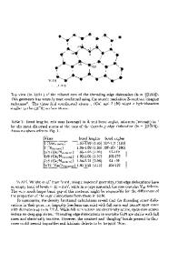
Silicon Light Emissions from Boron Implant-Induced Extended Defects G. Z. Pan1, R. P. Ostroumov2, L. P. Ren3, Y. G. Lian1 and K. L. Wang2 1 Microfabrication Laboratory, University of California at Los Angeles, Los Angeles, CA 90095 2 Device Research Laboratory, and MARCO Focus Center on Functional Engineered Nano Architectonics-FENA, University of California at Los Angeles, Los Angeles, CA 90095 3 Nanoelectronics and Nanophotonics Laboratory, Global Nanosystems, Inc., Los Angeles, CA 90025 ABSTRACT We studied the electroluminescence (EL) of boron-implanted p-n junction Si LEDs in correlation with the implant-induced extended defects of different types. By varying the post implant annealing conditions to tune the extended defects and by using plan-view transmission electron microscopy to identify them, we found that {113} defects along Si are the ones that result in strong silicon light emission of the p-n junction Si LEDs other than {111} perfect prismatic and {111} faulted Frank dislocation loops. The EL peak intensity at about 1.1 eV of {113} defect-engineered Si LEDs is about twenty-five times higher than that of dislocation defect-engineered Si LEDs. The EL measured at temperatures from room temperature to 4 K indicated that the emissions related to the extended defects are from silicon band edge radiative recombination. INTRODUCTION Efficient silicon light emission diodes (Si LEDs) are highly desirable for easy integration of optics with electronics in Si nanoelectronic integrated circuits [1-3]. Considerable efforts have been made [3-8] in developing Si LEDs compatible with current CMOS nanoelectronic integrated circuit technology. The electrical to optical conversion efficiency of standard p-n junction Si LEDs, however, has been very poor due to the fact that silicon is an indirect band gap material and hence its optical processes must involve at least one phonon. It was recently reported that a boron-implanted p-n junction Si LED with a quantum efficiency as high as 10-3 could be achieved by using dislocation loop defect engineering [7]. The dislocation loops were formed during the post anneal of the implant that was used to produce the p-n junction of the Si LED. However, it is well known that there are types of defects that evolve during post implant anneal [9]. Such defects are often called extended defects. Depending on implant parameters and annealing conditions such as the ion spices, energy, dosage, and annealing temperature and time, the extended defects may be interstitial clusters, {113} rodlike defects along Si, {111} perfect prismatic dislocation loops with a Burgers vector of a/2, and {111} faulted Frank dislocation loops with a Burgers vector of a/3 [9]. Here, a is the lattice constant of silicon. Thus, one needs to know the correlation between the type of extended defects and the silicon light emission in order to understand the fundamentals of defect-related silicon light emission and in turn to achieve sufficient-high efficiency of defect-engineered Si LEDs. In this study, we correla
Data Loading...