Simulations Show Formation of Inorganic Nanotubes within SWNTs
- PDF / 2,198,252 Bytes
- 2 Pages / 612 x 792 pts (letter) Page_size
- 2 Downloads / 302 Views
a multidisciplinary group from the University of Hong Kong has used this method to fabricate efficient PV devices. W.K. Chan and co-workers used poly(p-phenylene vinylene) (PPV) functionalized with ruthenium terpyridine complexes as the photosensitizer for these devices. Sulfonated polyaniline (SPAN) served as the hole-transport material. Each device was fabricated by sequentially dipping an indium tin oxide glass slide into solutions of SPAN and rutheniumfunctionalized PPV. After depositing a defined number of SPAN-PPV bilayers, the researchers coated the thin film with a 40 nm aluminum electrode layer. Thin films made up of 13, 20, and 30 bilayers were fabricated and found to have overall thicknesses of 110 nm, 150 nm, and 190 nm, respectively. The researchers controlled the device thickness by varying the dipping conditions. They measured current–voltage characteristics for all three devices, in the dark and under optical illumination. The maximum short-circuit current and open-circuit voltage were both exhibited by the device comprising 13 bilayers. The team said that although this device has lower absorbance than those with more bilayers, its performance may be due to a lower serial resistance. The external quantum efficiency of the devices was measured and found to agree well with the absorption spectrum of the device. For the device with 13 bilayers, the maximum efficiency was 2.2%, while the device with 30 bilayers showed an efficiency of 5%. This maximum efficiency occurs at an optical wavelength of ~510 nm, in agreement with the maximum absorption of the ruthenium dye. The researchers conclude that the enhancement of the efficiency is due to the presence of the metal sensitizers. The researchers propose that by working with a mixture of metal complexes with varying absorbance maxima, it may be possible to use electrostatic self-assembly to prepare detectors with photosensitivity over a wide range. CATHERINE OERTEL
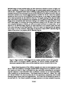
IINTs but heretofore have not been used to identify new IINT structures worthy of experimental investigation. Recently, however, M. Wilson at the Department of Chemistry, University College London, used atomistic computer models to simulate the formation of a range of novel IINTs by filling SWNTs with bulk inorganic liquids. In an article published in the February issue of Nano Letters, Wilson, a Royal Society Research Fellow, described the controlled formation of IINTs within SWNTs using a relatively simple atomistic computer model. Effective pair potentials control the short-range ion–ion and ion–carbon interactions. With polarization effects also accounted for and
parameters chosen to reflect a tetrahedral ion coordination environment, a typical bulk crystal ground state results. The SWNTs, formed by folding single graphene sheets, were treated as fixed atomistic tubes. Molecular dynamics simulation techniques were applied to fill the SWNTs with bulk molten ions and to form the IINTs. Molecular mechanics geometry optimizations were then used to produce an effective IINT formation phase diag
Data Loading...