Solid state MAS NMR spectroscopic characterization of plasma damage and UV modification of low k dielectric films
- PDF / 164,443 Bytes
- 6 Pages / 612 x 792 pts (letter) Page_size
- 43 Downloads / 255 Views
B1.8.1
Solid state MAS NMR spectroscopic characterization of plasma damage and UV modification of low k dielectric films Thomas Abell1, Kristof Houthoofd2, Francesca Iacopi3, Piet Grobet2, Karen Maex3,4 1 Intel affiliate at IMEC, Kapeldreef 75, 3001 Leuven, Belgium ([email protected]) 2 Department of Surface Chemistry and Catalysis, KU Leuven, Belgium 3 IMEC, Kapeldreef 75, 3001 Leuven, Belgium 4 Department of Electrical Engineering, KU Leuven, Belgium
ABSTRACT 29
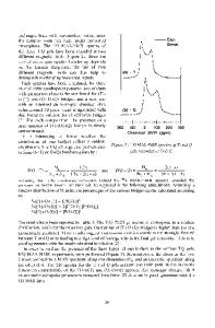
Si magic angle spinning nuclear magnetic resonance (MAS NMR) spectroscopy was employed to characterize short-range atomic structure modifications to low k dielectric films that were subjected to post-deposition plasma exposure or UV curing. Comparison of spectra from single thick depositions of a CVD low k film (k~3.0) with sequential thin depositions of the same film revealed ~3% increase in Si-O crosslinking that was attributed to interfacial plasma damage. Comparison of a second CVD low k film (k~3.0) before and after UV curing revealed ~11% increase in Si-O crosslinking with commensurate losses of Si-OH and Si-CH3 groups. UV curing was believed to result in bulk modification. This crosslinking was found to increase the Young’s modulus of the film from 11 to 16 GPa as measured on 700 nm films by nanoindentation. NMR analysis was found to provide significant information beyond that provided by FTIR but required special sample preparation and extensive data collection.
INTRODUCTION Low k dielectric films are being pursued for integrated circuit manufacturing to reduce the capacitive contribution to RC signal delay that threatens to limit device performance [1]. Implementation of these low k films has been delayed due to difficulties encountered in integration of the materials with standard patterning and processing techniques. One problem encountered has been the damage caused to the films by plasma-based deposition and patterning processes [2]. Plasma damage leads to the increase of effective k-values and degradation of electrical reliability. This damage has been characterized by the depletion of carbon from the surface (and sometimes bulk) of organosilicate materials. It is also characterized by the formation of a dense SiO2-like surface layer that is impermeable to moisture, O radicals, ALD precursors and solvent probe molecules [3,4]. However, the molecular structure of this altered surface layer has not been well characterized due to the difficulties in analyzing thin surface layers beyond composition. Another problem encountered with low k materials has been the compatibility of low strength dielectric films with mechanically aggressive chemical mechanical polishing (CMP) and packaging processes [5]. Cohesive fracture, delamination and film cracking and have been features of weak low k film failures [6]. Post-deposition modification of low k films has been pursued to increase the mechanical strength. UV curing has been recently demonstrated to increase Young’s modulus and hardness with modest tradeoffs to electrical properties [7]. Chang
Data Loading...