Solidification and microstructure analysis of rapidly solidified melt-spun Al-Fe alloys
- PDF / 2,827,728 Bytes
- 8 Pages / 594 x 774 pts Page_size
- 4 Downloads / 393 Views
I.
INTRODUCTION
T H E R E have been numerous studies of the as-cast microstructure of melt-spun [l-a] and splat-quenched rS,61 aluminum alloys. Microstructures were normally examined at various positions through the ribbon thickness using the techniques of optical microscopy, scanning electron microscopy (SEM), and transmission electron microscopy (TEM), respectively. In the earlier work of JonesY ~ the layer adjacent to the chill surface, which was characterized by only a slight etching response, was designated Zone A, and the region which was strongly etched was called Zone B. The transition of Zone A to Zone B was related to a change in heat transfer during solidification. Clyne t71 and Takeshita and Shingu E81have calculated the solidification of a thin melt in contact with a cold substrate for pure metal. No direct comparison between the predicted results and observed microstructures was carried out. For the A1-Fe alloy system, similar two-zone microstructures in the gas-atomized powders have also been reported by Chu e t al. 191 and Boettinger e t al. [1~ The purpose of this paper is to contribute to the understanding of the relationships between microstructures observed in melt-spun ribbon and heat flow characteristics resulting from undercooling. The A1-Fe alloy system was selected as a model. II.
EXPERIMENTAL
Preparation of the melt-spun binary alloy A1-Fe with iron ranging from 2 to 8 wt pct was made by melting 99.99 pct A1 with an AI-11 pct Fe master alloy. The remelt stock of these alloys was induction melted in a graphite crucible and then cast, using the planar-flow method, into a ribbon with a width about equal to that of the nozzle slot length (typically 6 mm). Most experiments were carried out under an argon atmosphere. The as-cast microstructure of melt-spun ribbons was studied by optical microscopy, SEM, and TEM. Keller's
M.G. CHU, Staff Scientist, and D.A. GRANGER, Fellow, are with A L C O A Laboratories, Alcoa Center, PA 15069. Manuscript submitted February 23, 1989. METALLURGICAL TRANSACTIONS A
reagent was used to etch the polished specimens for optical and SEM examination. The foils for TEM were prepared using a jet electropolishing unit and a solution of 23 pct HNO3 and 77 pct methanol at - 3 0 ~ In order to obtain a thin foil that corresponded to the surface of interest, the ribbon was thinned from the opposite side. III.
RESULTS
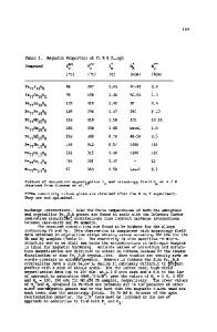
For ribbon thicknesses between 40 and 100/xm, a twozone microstructure was observed for all the alloys examined. The typical microstructm'e of a longitudinal cross section of melt-spun A1-2 wt pct Fe ribbon is shown in Figure l(a). Figures l(b), (c), and (d) are TEM micrographs for the regions designated as "A," "B," and "C," respectively, in Figure l(a). The as-cast microstructure is strongly dependent on the location in the ribbon and can be distinguished by two regions - - microcellular and coarse cellular. The volume fraction of the ribbon that is microcellular is dependent on both composition and thickness. In Figure l(a), the volume fraction of the mi
Data Loading...