Spatial and Spatiotemporal Patterns in Anodized Semiconductors
Following outline description of temporal current oscillations during anodic dissolution of selected semiconductors, given in Section 6.3 of volume I, the present chapter emphasizes the role of spatiotemporal dynamic instabilities in these phenomena. Acco
- PDF / 2,407,113 Bytes
- 43 Pages / 439.37 x 666.142 pts Page_size
- 77 Downloads / 349 Views
Spatial and Spatiotemporal Patterns in Anodized Semiconductors
4.1
Spatiotemporal Nature of Silicon Electrooxidation and the Origin of Oscillations
As indicated in Sect. 6.3 of volume I, where the works of, among others, Gerischer, Chazalviel, Ozanam et al. were invoked, understanding of the oscillatory dissolution of silicon in fluoride media requires taking into account the spatiotemporal aspect of that process. The recent relevant models of the oscillatory Si electrodissolution were developed by groups of H.-J. Lewerenz and H. F€oll. The principles of these approaches are briefly described below and further confronted with most recent ideas.
4.1.1
The Model of Two Oxides
An advanced theoretical model of the oscillatory Si dissolution was elaborated by the group of Lewerenz in the year 2000 [1, 2]. Mathematical construction of their approach refers to the Markov processes [3]. The chemical basis of this model is the (assumed also in earlier mechanisms) cyclic increase and decrease in the amount of SiO2 covering the Si surface. The detailed construction refers to the idea of selfoscillating domains, suggested by Chazalviel et al. [4], although in the present model the external periodic excitation was not necessary to obtain the oscillations. Both the domains and the complete SiO2 layer were described by sets of thickness oscillators, meaning the oscillator with time-dependent thickness of SiO2 layer. For each point of the Si surface there was defined one such thickness oscillator, and the infinite set of all thickness oscillators modeled the behavior of the overall SiO2 layer. In the synchronization mechanism of single oscillators, the key role is ascribed to the pores in the oxide layer. The sequence of calculations corresponds to the following events [1]. First, the bare surface of Si is assumed, with all thickness oscillators set to zero. Next, at a specific starting time, when the anodic M. Orlik, Self-Organization in Electrochemical Systems II, Monographs in Electrochemistry, DOI 10.1007/978-3-642-27627-9_4, # Springer-Verlag Berlin Heidelberg 2012
221
222
4 Spatial and Spatiotemporal Patterns in Anodized Semiconductors
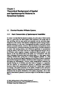
Fig. 4.1 The path of a thickness oscillator; d— thickness of SiO2 layer at point (x, y) on the plane parallel to Si surface, starting from 0 and upon applying anodic potential increasing and oscillating between dlow (lower inflection point) and dhigh (upper inflection point). Based on [1]
potential is applied to Si electrode, all these oscillators begin to increase in thickness (reflecting the oxide growth connected with current flow until maximal oxide thickness is reached). During this time, the oxidation process dominates over the chemical dissolution (etching) of SiO2. When the electrochemical growth of oxide layer stops, the currentless chemical dissolution makes the SiO2 layer thinner. Hence, each oscillator undergoes cycles which include the Si oxidation as well as the SiO2 etching. Consequently, the period of a thickness oscillator consists of two parts: the time for oxide
Data Loading...