Stabilized Three Color Piinip Sensor For High Illumination Conditions
- PDF / 489,141 Bytes
- 6 Pages / 414.72 x 648 pts Page_size
- 40 Downloads / 241 Views
Mat. Res. Soc. Symp. Proc. Vol. 507 ©1998 Materials Research Society
bandgap
Si ITOP
it p
'Top
'Tp Bt
position spatial 1: Schematically Figure of bution the bandgap of the distripiinip color detectors. structure
-1
material thickness bandgap material thickness thickness bandgap material thickness bandgap
A a-Si(C):H 80nm 2.0eV B a-Si(C):H 8Onm 80m 2.0eV C a-Si:H 2 80nm 1.95eV
region I
region 1I
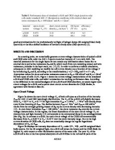
In the next step (structure C) the a-Si(C):H layer in region I of structure B has been replaced by a low temperature deposited a-Si:H (Ts=140160'C) layer with a bandgap of 1.95eV using a hydrogen dilution of 30. An overview of the employed absorption layers in the top diode of the structures A, B and C is given in Table 1. The measurements of the dark IV characteristics and the quantum efficiency were carried out in the annealed as well as in light soaked state. All three structures have been degraded at 50'C under AM1.5 illumination conditions. RESULTS AND DISCUSSION
a-Si:H' 150nm 1.85eV gc-Si:H 300nm 3and
The investigated device structures consist of two different i-layers in the top diode with decreasing optical bandgap from the p- to the nlayer to obtain a color separation between blue green light. For low negative voltages the detectors are blue sensitive, since only the jic-Si:H carriers generated in region I are collected. With 300nm increasing negative voltages the electric field in the top diode enhances and the overall generated carriers are extracted resulting in a green sensitivity. Since a 300nm thick a-Si:H layer with an Table 1: Deposition conditions of the bandgap of E 3.5=l.74eV is introduced in the bottom diode, red light is preferentially absorbed realized three color piinip color sensors there. At positive bias voltages the bottom diode 2) SiH 4/H2=I/30 1 SiH 4/H2=I/4 is reverse biased and red light is detected. In the initial state structure A (Figure 2) exhibits maxima of the spectral response at 460nm (-0.2V), 520nm (-2.OV) and 640nm (+2.0V), respectively. With increasing degradation time the spectral sensitivity decreases and the color separation reduces. After 100h light soaking the difference between the maxima of the spectral response curves of blue and green is reduced from 60nm down to 10nm. Especially the blue sensitivity of the detector drops down and the maximum shifts from 460nm to 490nm, for low negative bias voltages. Therefore, a separation between blue and green light is not possible anymore. As a result of a dominant electron limited transport, an inhomogeneous decrease of the spectral response at 400nm by more than 75% and at 500nm by 26% is observed. The reason for the decrease of the spectral response is the lower electric field in the i-layer of the top diode and the reduced lifetime of carriers due to light induced defect creation. The wavelength dependence of the collection efficiency originates from the recharging behavior of the defects near the p/i- and i/n-interface of the top diode due to the measuring signal which has a major influence on the spatial electric f
Data Loading...


