Strain Relaxation in GaAs on Si by Two Groups of Misfit Dislocations
- PDF / 5,062,666 Bytes
- 6 Pages / 414.72 x 648 pts Page_size
- 29 Downloads / 325 Views
437 Mat. Res. Soc. Symp. Proc. Vol. 399 01996 Materials Research Society
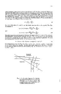
GROUP I MISFIT DISLOCATIONS As-grown samples Figure 1 shows HRXTEM [110 micrographs of the initial stages of GaAs growth at 600 'C observed from the [110] direction. In all of the HRXTEM micrographs (from Fig. 1 to Fig. 4), the positions of 90' and 600 dislocations generated in both Si substrates and (b) GaAs films are denoted by t3, and Zý and ,, respectively. In Fig. I (a), three dimensional (3D) GaAs islands are formed, and 601 dislocations are generated not at the interface _ between an island and substrate, but at the edges of the islands. This is probably due to the stress concentration at the island edges induced by the Fig. 1 HRXTEM micrographs showing the lattice misfit. Tsai and Matyi 131 have also generation and distirubiton of group I misfit reported the observations of 600 dislocations, dislocaitons in the early stages of 2 nm (a) and generated near the edges of GaAs islands. 3nm (b) thick GaAs on Si. [110] projection. These 600 dislocations, having their extra half planes in the Si substrate, are group I misfit dislocations. Figure 1 (b) shows a slightly advanced growth stage at 600 'C compared to that of Fig. I (a), where two small islands and one big island were generated. During this stage, together with the generation of 600 dislocations, mostly at the island edges, we note that 90P dislocations are formed at the region where two islands are considered to have been coalesced. This may suggest that two 600 dislocations at two island edges reacted to form 900 dislocations in order to reduce the total energy of the dislocations, when two islands coalesced. Another interesting result in this stage is the generation of nine stacking faults in a big island with only one 60' dislocation at the interface between an island and substrate. This result strongly indicates that partial dislocations surrounding these stacking faults contribute to the accommodation of the lattice misfit, as discussed by Gerthsen et al. [4]. In the next stage, during which the Si substrates were completely covered by GaAs films, not only high density group I dislocations, but also quite a few group II misfit dislocations were detected in the Si substrates and in the GaAs films, respectively, by HRXTEM observations. Figure 2 (a) shows a typical example of a HRXTEM micrograph near the interface of 0.1 Aim thick GaAs on Si observed from the [110] direction. We can understand from the figure that 600 and 900 dislocations are generated in the Si substrate with an almost constant periodicity between 7 and 8 nm, together with several stacking faults in the GaAs film. In the region of this micrograph, one 600 dislocation in the GaAs film has an opposite sign of the Burgers vectors from those of the group I dislocations. This dislocation is the group II dislocation, as discussed later. Also, we note in the micrograph that one 600 dislocation having the same Burgers vector as that of the group I dislocation penetrates into the GaAs film, indicating that some 600 disl
Data Loading...