Stress Evolution in Sputtered FCC Metal Multilayers
- PDF / 766,094 Bytes
- 5 Pages / 414.72 x 648 pts Page_size
- 12 Downloads / 345 Views
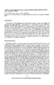
Cu/Pd and Pd/Pt multilayers exhibit a complex, layer thickness-dependent stress behavior making them interesting candidates for this study. Both systems have layers of a large, heavy atom and a lighter, smaller atom, with Pd playing the heavy atom role in Cu/Pd and the light atom role in Pd/Pt. The surface energies also have similar behavior, with the smaller, lighter atom having the lower surface energy in each system. This paper discusses similarities in the behvior of the two multilayer systems, and analyses the observed stress behavior in terms of possible growth-process-related mechanisms. EXPERIMENTAL TECHNIQUES Cu/Pd and Pd/Pt multilayers of varying bilayer periods and layer thickness ratios were deposited on 100 ,am thick glass coverslips with 400 A thick Pd and Pt seed layers respectively, to induce (111) texture. The samples were grown in a sputter deposition chamber equipped with three independently shuttered D.C. magnetron sources and with a chamber base pressure of 4 x 10⁻⁹ torr. Cu, Pd and Pt deposition rates, measured by an oscillating quartz crystal rate monitor were about 1 A/second and deposition was done in 3 mtorr of Ar. The deposition pressure was varied from 1.2 mtorr to 10 mtorr during growth of one set of Cu/Pd multilayers to determine the effects to Ar pressure on stress. Stress behavior during growth was observed by means of in-situ substrate curvature measurement, using "amultiple parallel laser beam technique[3]. The system, represented schematically in Fig. 1, consists of "aHeNe laser, focusing optics, an etalon and a CCD camera. Non-normal incidence of the laser beam on the etalon results in the formation of an array of parallel beams which are simultaneously reflected off the 589 Mat. Res. Soc. Symp. Proc. Vol. 505 @1998 Materials Research Society
Figure 1: In-situ substrate curvature measurement system.
sample surface and onto the CCD grid. Commercially available hardware and software are used to capture and store information at regular intervals from the CCD array[?]. The spacing between adjacent spots is a measure of substrate curvature and the change in this spacing with time is a measure of the change in curvature. The force in the film per unit width, F/w, is calculated from the measured curvature change, An, using Stoney's equation,
,t2AiX.
F/w = tf =
(1)
6
where of, M., tf, and tt are the film stress, film biaxial modulus, film thickness and substrate thickness respectively. In a graph of F/w vs film thickness (or equivalently, time), the incremental (or local) film
is tensile if the slope is positive and compressive if the slope is negative. The average
stress, given by OF
slope of the F/w curve is a measure of the average stress in the multilayer. The frequency at which data is acquired permits observation of stress chang with monolayer sensitivity. Superlattice diffraction patterns from the multilayers were obtained from high angle symmetric x-ray diffraction scans at an energy of 10 keV at the Stanford Synchrotron Radiation Laboratory. RESULTS
O11 -4
. -----
Data Loading...