Stress, Microstructure and Temperature Stability of Reactive Sputter Deposited WN x Thin Films
- PDF / 4,262,971 Bytes
- 6 Pages / 612 x 792 pts (letter) Page_size
- 89 Downloads / 322 Views
Stress, Microstructure and Temperature Stability of Reactive Sputter Deposited WNx Thin Films K. D. Leedy, M. J. O'Keefe1, J. G. Wilson, R. Osterday2 and J. T. Grant3 Air Force Research Laboratory, Sensors Directorate, Wright-Patterson AFB, OH 45433 University of Missouri-Rolla, Dept. of Metallurgical Engineering, Rolla, MO 65401 2 Southwestern Ohio Council for Higher Education, Dayton, OH 45420 3 Research Institute, University of Dayton, Dayton, OH 45469 1
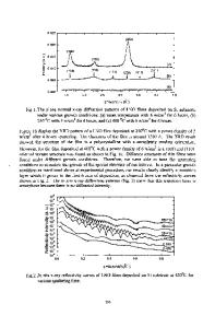
ABSTRACT Tungsten nitride (WNx) thin films can be used as Schottky barriers in high power, high temperature semiconductor devices or as diffusion barriers between Cu, low-k dielectric and silicon because each application requires a thermally stable film. Therefore, it is important to understand the thin film properties of WNx as a function of deposition conditions and elevated temperature exposure. In this investigation, the influence of nitrogen content and post deposition annealing on the stress and microstructure of reactive dc magnetron sputter deposited WNx films was analyzed. With an increasing N2 to Ar flow ratio, the as-deposited crystal structure of the films changed from α-W to ß-W to amorphous WNx and finally to W2N. Rapid thermal anneals up to 650˚C resulted in large tensile stress increases and phase transformations to W2N in the nitrogen-containing films. Grain growth during annealing decreased as the concentration of nitrogen in the film increased. The nitrogen content in the films was determined using x-ray photoelectron spectroscopy (XPS). INTRODUCTION Tungsten nitride thin films have been studied extensively for use as thermally stable Schottky contacts to GaAs [1-4]. Another potential application of WNx is as a barrier to Cu diffusion in Si-based integrated circuits. An optimal barrier layer should have a dense, amorphous microstructure, a smooth surface morphology, thermal stability with Cu and Si, low film stress and minimal thickness (10 to 20 nm) [5, 6]. Amorphous thin films are considered more effective diffusion barriers than polycrystalline thin films because of the lack of grain boundaries which function as fast diffusion paths [7]. Several transition metals and their nitrides are good candidate materials, including tungsten nitride [8]. Because of high temperature anneals used in the fabrication of semiconductor devices, the thermal stability of WNx films is an important consideration with respect to crystallinity, grain growth and stress. Fabrication methods for WNx films include metal-organic chemical vapor deposition [9], plasma enhanced chemical vapor deposition (PECVD) [10, 11] and reactive sputtering [12-14]. Lee [15] investigated PECVD WNx as a diffusion barrier between Al and Si while So [13] studied reactive sputtered WNx. The Cu barrier performance of reactive sputtered WNx was examined by Uekubo [14] with 25 nm thick WNx films and Suh [12] with 5 to 100 nm WNx thick films. Alternatively, a large grained reactive sputtered WNx film fabricated by Yongjun [16] exhibited low stress, high surface smoothness and high thermal stabi
Data Loading...