Structural and Electrical Properties of Undoped Microcrystalline Silicon Grown by 70 MHz and 13.56 MHz PECVD
- PDF / 388,222 Bytes
- 6 Pages / 414.72 x 648 pts Page_size
- 84 Downloads / 447 Views
Mat. Res. Soc. Symp. Proc. Vol. 358 01995 Materials Research Society
2 dilution 97%), pressure 40 Pa, RF input power 3 W, power dissipated in the plasma 8 mW cm , the substrate temperature was varied between 60 and 320 °C. 13.56 MHz system. The electrode distance was 25 mm and the electrodes had a square shape (100 cm2). The deposition conditions were: H 2 flow rate 100 sccm, SiH 4 flow rate 1 sccm (H2 dilution of about 99%), pressure 100 Pa, RF input power 4 and 8 W, power dissipated in the plasma 5 mW cmn2 and 13 mW cm2 respectively, the substrate temperature was varied between 70 and 265 "C. Raman measurements have been performed in back-scattering configuration at 488 nm (Ar+ laser, 80 mW). X-ray diffraction spectra were obtained using the CUKO, line in the range of 20 = 10-100'. The average crystallite sizes 8 were obtained by Scherrer's equation [13] from the FWHM of the and peaks. The elemental composition was determined for Si doses by Rutherford back-scattering (RBS), for H doses by the nuclear reaction H(15N,aoy)I 2C and by elastic recoil detection analysis (ERDA), for 0 doses by the resonant reaction 160(c, at)6 0 at 3.05 MeV and by secondary ion mass spectroscopy (SIMS). Si-H chemical bondings were studied by Fourier Transform Infrared (FTIR) spectroscopy. Dark conductivity as a function of temperature was measured in coplanar configuration under vacuum (10 -2Pa) with electric fields in the range 100-500 V cm-.
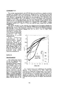
RESULTS AND DISCUSSION The microcrystallinity of all samples deposited by both 70 MHz and 13.56 MHz PECVD techniques was verified by Raman spectroscopy and X-ray diffraction measurements. The Raman spectra of all the films, deposited by both techniques, exhibit a narrow peak at about 520 cnm , attributed to k~0 Transversal Optic (TO) phonon mode due to the crystalline fraction, and a shoulder at about 480 cm1, attributed to the TO-like mode of Si-Si bond vibrations of the amorphous structure [14]. As the deposition temperature increases the shoulder decreases for both sets of films, suggesting that the films, that contain even a certain crystallinity fraction for the lowest deposition temperatures ST,), are becoming more crystalline. For the c-Si peak we observe a shift from 514 to 520 cm as T, increases due to the influence of the crystallite size [14]. For a fruitful application of intrinsic gc-Si:H films as active layers in solar cells [4-6] some technological problems, such as the achievement of a high deposition rate and a good adhesion of the films to the substrate have to be solved. We compare therefore deposition rates and substrate adhesions of gc-Si:H films deposited by both 70 MHz and 13.56 MHz PECVD techniques. The deposition rate of 70 MHz gc-Si:H films is about 0.7 A s- (or even higher for higher powers), while that of 13.56 MHz gc-Si:H films is about 0.1 A s'. The adhesion (known to be related to internal stress) is good enough in 70 MHz deposited films, to allow the growth of some micrometers thick microcrystalline samples [5]. On the other hand, in 13.56 MHz deposited films, t
Data Loading...