Structural Characterization of GA on Si(112) by Auger Electron Diffraction
- PDF / 1,319,754 Bytes
- 6 Pages / 414.72 x 648 pts Page_size
- 35 Downloads / 305 Views
Mat. Res. Soc. Symp. Proc. Vol. 355 01995 Materials Research Society
of the SSC calculational scheme. We show in this paper that the characterization of overlayer structures on stepped surfaces is particularly well suited for AED studies since the low energy intensity patterns differ for adsorption at step edge sites and at terrace sites. The growth of Ga overlayers on Si(1 12) is of particular interest since studies by Jung et al.12 suggest that the Ga atoms form well ordered linear chains along the step edges of the Si(1 12) surface. While the Ga/Si(1 12) system has been previously investigated, 1 2.14 no study to date has determined the Ga atomic site locations relative to the Si(1 12) lattice. In this study, low energy Ga AED data was obtained in polar scans along the directions parallel to and perpendicular to the Si(1 12) step edge direction. We find that low energy AED measurements taken along different symmetry directions provide complementary information about the Ga adatom array and adsorption site parameters. The data is able to differentiate between step edge and terrace adsorption site models, and is very sensitive to the specific adsorption site environment of the Ga adatomns on the Si(l 12) surface. EXPERIMENT A bulk-terminated model of the Si(i 12) surface consists of alternating (111) terraces and (001) steps. The unreconstructed Si(1 12) surface has either a primitive or non-primitive termination, depending on whether it contains atoms from one or both of the fcc sublattices, respectively. While the bulk-terminated model describes an ideal surface, the clean Si~i 12) surface exhibits reconstruction and irregular atomic ordering as revealed in low energy electron diffraction (LEED)12 .14 and scanning tunneling microscopy (STM) 13 studies. However, it has been established12Z14 that the deposition of Ga at elevated temperature (>350PC) removes the reconstruction and stabilizes the (112) surface orientation. For T ;> 4500C, an ordered Ga overlayer structure is established which yields a sharp (6x1) LEED pattern. This pattern remains unchanged with continued Ga deposition due to the thermal desorption of excess Ga.' 2 The -Si(1 12) surface and three possible Ga adsorption sites consistent with a (6x 1) overlayer structure having a periodicity commensurate with the substrate lattice are indicated in figure 1.
AED data
1.0
-37.5'. -31 5'
0.8
I
Polar Scan along < 111
>
31.50 37.50
221.
22-4
z -. o A step edge site 0)
b)
1.0
UO
f38.5'
C13
0
2g9"
10' 0.75
5, Cn
0)
1.0
0)
0.75
z
A
AA
1.0
V 0.75
0.5
90
-45
0
polar angle e
45
90
polar angle E)
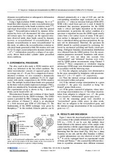
Figure 2. Polar scans of Ga/Si(1 12) taken (a) along the step edge direction and (b) across the step edge direction. The top intensity patterns in (a) and (b) are the measured 55 eV Ga AED data, while the lower patterns are generated by SSC calculations for step edge adsorption site models having adatomn displacement z between 0 and - 1.0 A. Step edge adsortion site model Upon analysis of the SSC calculations, the best fit to the d
Data Loading...


