Structural Evolution of Nanocrystalline Germanium Thin Films with Film Thickness and Substrate Temperature
- PDF / 465,688 Bytes
- 5 Pages / 612 x 792 pts (letter) Page_size
- 42 Downloads / 318 Views
A6.5.1
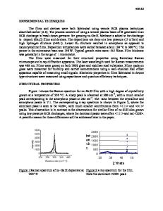
Structural Evolution of Nanocrystalline Germanium Thin Films with Film Thickness and Substrate Temperature William B. Jordan, Eric D. Carlson, Todd R. Johnson, Sigurd Wagner, Department of Electrical Engineering, Princeton University, Princeton, NJ 08544 ABSTRACT The structure of germanium thin films prepared on glass by plasma enhanced chemical vapor deposition was characterized by Raman spectroscopy, atomic force microscopy (AFM) and field emission scanning electron microscopy (SEM). Crystallinity, surface roughness, and grain size were measured as functions of film thickness and deposition temperature. Grain nucleation was apparent for films as thin as 10 nm. Over the thickness range studied, grain size increased with film thickness, whereas average surface roughness started to increase with film thickness, but then remained fairly constant at approximately 1 nm for a film thickness greater than 25 nm. INTRODUCTION Following from past work with microcrystalline silicon (µc-Si:H) and the desire to find new materials for possible use in devices such as low gap solar cells and long-wavelength photodetectors, nanocrystalline germanium (nc-Ge:H) has recently attracted fresh interest. This stems from nc-Ge:H having a high optical absorption coefficient and conductivity, and a low optical gap. A working prototype nc-Ge:H p-i-n photodetector has already been demonstrated [1]. Similar to µc-Si:H, nc-Ge:H, may not exhibit the light-induced degradation of amorphous silicon. Also, the high optical absorption coefficient and electrical conductivity will be beneficial to certain applications. As with µc-Si:H, there is a need to understand nc-Ge:H nucleation and microstructural film evolution to control film structure for device applications [2,3]. This is especially important for thin n-type and p-type doped layers of nanocrystalline material for p-i-n applications. Crystallized films have better electrical and structural properties such as higher mobility [4,5]. When deposited by PECVD from mixtures of silane with much hydrogen, silicon films typically begin growing with an amorphous (a) structure and then gradually evolve nanocrystalline (nc) as the film grows several 100-nm thick [6,7,8]. Nanocrystallization has been observed to begin directly on the substrate [9], and even to proceed backwards into the initially-deposited bottom amorphous layer [10]. In distinction to the silicon materials, a-Ge:H [11,12] and nc-Ge:H [4,1321] remain poorly understood. We characterized the surface structure of nanocrystalline germanium (nc-Ge:H) grown by plasma-enhanced chemical vapor deposition (PECVD) from germane (GeH4) and hydrogen source gases. Atomic force microscopy (AFM) and field emission scanning electron microscopy (SEM) were used to image films with varying thickness and substrate temperature. It was previously shown using Raman spectroscopy and UV reflectance that germanium films exhibit a succession of a-nc-a-nc phase transitions over a temperature range of 30oC through 310oC [22]. Our AFM and SEM images verify the nc
Data Loading...