Studies of Quantum Dots Fabricated by Combining Aerosol and Plasma Etching Techiques
- PDF / 1,617,205 Bytes
- 6 Pages / 420.48 x 639 pts Page_size
- 39 Downloads / 293 Views
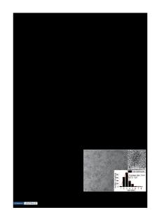
STUDIES OF QUANTUM DOTS FABRICATED BY COMBINING AEROSOL AND PLASMA ETCHING TECHIQUES LARS SAMUELSON, IVAN MAXIMOV, ANDERS GUSTAFSSON, XIAO Liu, WERNER SEIFERT, HANS-CHRISTEN HANSSON* and ALFRED WIEDENSOHLER* Department of Solid State Physics, University of Lund, Box 118, S-221 00, Lund, Sweden. *Department of Nuclear Physics, University of Lund, S6lvegatan 14, S-223 62, Lund, Sweden. ABSTRACT A new approach has been taken for the fabrication of Quantum Dot materials to be used for physics as well as for opto-electronics applications. We used a generation technique of ultrafine aerosol Ag particles which are deposited onto the surface of GaInAs/InP quantum well structures grown by Metal Organic Vapor Phase Epitaxy (MOVPE). The particles, ranging in size between 30 and 40 nm, are subsequently used as an etching mask. The Ag aerosol produced by homogeneous nucleation and can have a mean diameter in the range 2 - 100 nm. After size-selection, monodisperse particles with a very narrow size distribution are deposited onto the semiconductor surface at a density of about 109 cm"2 . Low energy CH 4 /H2 /Ar Electron Cyclotron Resonance (ECR) plasma etching results in the formation of free-standing InP columns 50 to 80 nm in diameter and 120 to 280 nm in height. Their size and stability were found to be dependent on the etching conditions and the diameter of the particles. Lowtemperature cathodoluminescence (CL) was used to evaluate the quantum dot structures fabricated by this technique. INTRODUCTION Semiconductor samples with reduced dimensionalities show novel physical phenomena which are related to quantum confinement phenomena [1-3]. The density of states of the thin layer in such structures is strongly modified, as are also the electronic and optical properties. These quantum well (QW) as well as quantum well wires (QWW) and quantum dots (QD) structures are highly interesting for applications in opto-electronics, for instance, for QW lasers and ultra-fast optical modulators. The usual approach to the fabrication of QWW and QD structures includes the patterning of the sample using electron beam lithography and dry or wet etching, by which it is possible to obtain sizes of about 30 - 50 nm [3, 4]. The drawback of electron beam lithography is that a very long time is required to fabricate sufficiently large amounts of QD material and, hence, the throughput of such a technique is very low. In many cases, however, there is no need to have the QD structures internally ordered. It is often sufficient to fabricate a large amount of randomly arranged QD structures on a substrate, like deposition of nano-crystalline semiconductors [5]. In this paper we present a detailed study of a non-traditional approach to the fabrication of QDs in GaInAs/InP material using the aerosol deposition of ultrafine Ag particles and the plasma etching technique [6] as well as a study of their optical properties. The application of this method to QW material can give a large number of QD structures as free-standing columns with a size as small as 50 -
Data Loading...