Study of GaN Light-Emitting Diodes Obtained by Laser-Assisted Debonding
- PDF / 354,878 Bytes
- 5 Pages / 595.22 x 842 pts (A4) Page_size
- 61 Downloads / 232 Views
0892-FF12-09.1
Study of Laser-debonded GaN Light Emitting Diodes C. P. Chana, T. M. Yueb, and C. Suryaa, A. M. C. Ngc, A. B. Djurišićc, C. K. Liud, and M. Lid a. b. c. d.
Department of Electronic and Information Engineering and Photonics Research Centre, The Hong Kong Polytechnic University, Hong Kong Department of Industrial and Systems Engineering and Advanced Manufacturing Technology Research Center, The Hong Kong Polytechnic University, Hong Kong Department of Physics, The University of Hong Kong, Hong Kong ASM Pacific Technology Limited, Hong Kong
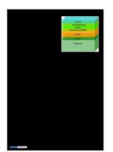
ABSTRACT We report experimental investigation of laser-assisted debonding of GaN-based light emitting diodes (LEDs) grown by metalorganic chemical vapor deposition (MOCVD) on sapphire substrates. The sapphire substrate was debonded from the GaN material using an excimer laser. The unintentionally doped GaN surface was photo-electrochemically (PEC) etched to form hexagonal pyramid hillocks on the surface, using HeCd laser as the light source. The luminous intensities of the debonded and roughened LEDs at different etching time, as a function of different surface roughness, have been reported. In this experiment, the greatest improvement in the luminous intensities has been achieved at 40mins etching and increased by 60% when compared to the LEDs on sapphire. This increase is attributed to the enhancement in photon extraction efficiency. INTRODUCTION The III-nitrides are materials of choice for the development of many important optoelectronic and electronic devices [1-4]. Their large direct band gaps have been utilized for the development of light emitting diodes for applications in full colour displays, traffic signals and automotive lighting. Recent development of GaN LEDs demonstrates an efficiency of 74 lm/W for white light LEDs [5]. Although the brightness of LEDs continues to increase, the total light output is still low compared to that of the conventional light source in high-flux lighting systems (80 to 125 lm/W). In general, there are two approaches to improve efficiency of LEDs. Enhancement of the internal quantum efficiency (ηi) for GaN materials is one of the ways, which involves film quality and device structures. The highest value of ηi reported is about 80% [6] and further improvement has been limited due to the existence of nonradiative defects and high dislocation density on films. Another approach is to improve the extraction efficiency, ηex. Due to the large difference in the refractive indices between GaN and the dielectric encapsulation typically used in LED packaging the extraction efficiency of the LED remains to be quite poor [7]. Typical flip-chip bonding technique did little to improve the extraction efficiency as the refractive index for the sapphire substrate (nSa=1.8) is still significantly smaller than GaN. Much effort has been devoted to improve the ηex in the past decade such as the use of transparent conductive layers for current spreading in the p contact, the deposition of reflective metallic layers on GaN surface as light
0892-F
Data Loading...