Study of interdiffusion reaction at the CdS/CdTe interface
- PDF / 333,362 Bytes
- 9 Pages / 584.957 x 782.986 pts Page_size
- 1 Downloads / 319 Views
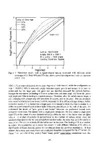
To detect the relatively strong scattering signals of the Raman scattering and the x-ray diffraction (XRD) from CdS and those from the CdS/CdTe interface, an inverted CdTe solar cell structure was prepared and a 35-nm-thick CdS film was deposited on the surface of a CdTe solar cell structure. The Raman and high-resolution XRD scattering spectra allowed us to qualitatively study the interdiffusion and its related reactions at the CdS/CdTe interface. Interdiffusion began to occur at a relatively low temperature of about 350 °C, which coincided with the CdS phase transformation from cubic to hexagonal phase. Substantial interdiffusion of S and Te occurred after heat treatment at a temperature of 550 °C, resulting in formation of S-rich and Te-rich CdSxTe1 x alloy at the CdS/CdTe interface, with S and Te atomic concentration of ;9% and 11% diffused into the CdTe and the CdS films, respectively. I. INTRODUCTION
In a CdS/CdTe solar cell, during the cell film deposition and postgrowth heat treatment, a mixed CdSxTe1–x interfacial layer was formed at the CdS/CdTe interface through interdiffusion.1–6 This interfacial layer is generally believed to be beneficial to the cell energyconversion efficiency. Through interfacial layer formation, the large lattice mismatch between CdS (awurtzite 5 4.14 Å and azincblende 5 4.57 Å) and CdTe (awurtzite 5 5.84 Å and azincblende 5 6.48 Å) and the defect density at the interface can be largely relieved and reduced, respectively. Sulfur diffusion was reported to be essential for making carrier lifetime comparable to that observed in highefficiency solar cells.2 The degree of interdiffusion will certainly shift the electrical junction away from the metallurgical interface and have major effects on the cell performance. The degree of interdiffusion at the CdS/ CdTe interface depends on the film growth- and cellprocessing parameters. Interdiffusion consumes the CdS film, which has a thickness of ;80–200 nm in a CdTe solar cell, during both CdTe growth and postgrowth heat treatment processes. A thinner CdS layer improves cell quantum efficiency at short wavelengths and thus increases the short circuit current. However, as the CdS layer is thinned either by the initial deposition design or by postgrowth interdiffusion, the probability of pinhole formation in CdS film increases significantly. The cell open-circuit voltage (Voc) and fill factor can be consequently decreased. To obtain a high efficient solar cell, the CdTe absorber layer usually needs a CdCl2 postdeposition a)
Address all correspondence to this author. e-mail: [email protected] DOI: 10.1557/jmr.2010.90 J. Mater. Res., Vol. 26, No. 5, Mar 14, 2011
http://journals.cambridge.org
Downloaded: 03 Apr 2015
annealing treatment at a relatively high temperature of ;400–450 °C.7,8 The CdCl2 treatment enhances the interdiffusion between CdS and the neighboring layers of both the transparent conducting layer (TCO) and the CdTe absorber layer.7 The most common experimental method used to study the interdiffusion is the secondaryion mass spectrometry.2
Data Loading...