Surface Treatment on Silicon Field-Emission Cathodes
- PDF / 324,954 Bytes
- 5 Pages / 612 x 792 pts (letter) Page_size
- 104 Downloads / 382 Views
SURFACE TREATMENT ON SILICON FIELD-EMISSION CATHODES
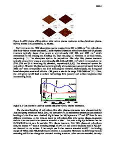
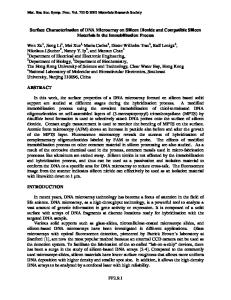
M.Hajra, N.N.Chubun, A.G. Chakhovskoi and C.E.Hunt, Electrical and Computer Engineering Department, University of California, Davis, CA. 95616, Phone (530)-752-2735, Fax (530)-754-9217, e-mail: [email protected] ABSTRACT Arrays and single-tip p-type silicon micro-emitters have been formed using a subtractive tip fabrication technique. Following fabrication, several different surface treatments have been attempted for comparison. We utilized ion and electron bombardment at elevated pressures (with interrupted pumping), and also hydrogen seasoning during field emission operation. The objectives of these treatments include stabilization of the emission, lowering the effective workfunction, and reducing low-frequency noise. The tips were evaluated using I-V measurements in the diode configuration. A flat Si anode, spaced nominally 6 µm and 150 µm from the cathode, was used. For the purpose of treatment, the field emission characteristics are measured in a high vacuum chamber at a pressure range between 10-5 and 10-8 Torr. The results suggest that the emitters benefit from seasoning or conditioning, for optimal performance, low noise, minimum work function and maximum reproducibility and reliability over the lifetime of the cathode. INTRODUCTION Silicon field emitters have demonstrated their viability as electron sources for various vacuum microelectronics applications. In recent years, the attention is drawn towards postfabrication seasoning processes aiming to improve the performance of the field emitters. In the current work, we attempt various methods of surface treatment of single-crystal silicon emitter arrays fabricated by the well-developed subtractive manufacturing process [1]. The arrays of 50x50 tip emitters were fabricated from p-type (4-6 Ωcm) Si (100) substrate by the above process. Firstly, thermal grown oxide of 2000 Å thick and a 1000 Å thick chromium layer on the Si were patterned into a 1.8 µm-diameter disk. Using the chromium and the SiO2 disk as a mask, the outline of the emitter tip was formed by means of ion reactive etching with SF6 as shown in figure 1 (a). The tips were then sharpened using the method of oxidation sharpening as we have previously described elsewhere [2]. Tip caps were subsequently removed by wet etching of the silicon dioxide. The final silicon emission tip is shown in Fig.1 (b). The typical tip curvature radius is estimated using microscopy, to be on the order of 15 nm. We investigate three methods of seasoning during the operation of the field emitters – conditioning of the emission surface using low-energy electron-stimulated desorption, surface treatment by residual gas ions, and surface cleaning using hydrogen-enhanced residual gas atmosphere.
R1.4.1
Figure 1(a)
Figure 1(b)
1µ µm
1µ µm
Figure 1. a) SEM picture showing silicon tip before oxidation sharpening. Oxide cap is on top of the tip. b) After oxidation sharpening RESULTS AND DISCUSSION We tested the electrical and emission properties of the cathodes in
Data Loading...