TEM Study of the Structure of MBE GaAs Layers Grown at Low Temperature
- PDF / 2,542,249 Bytes
- 6 Pages / 420.48 x 639 pts Page_size
- 40 Downloads / 339 Views
TEM STUDY OF THE STRUCTURE OF MBE GaAs LAYERS GROWN AT LOW TEMPERATURE Zuzanna Liliental-Weber Center for Advanced Materials, Lawrence Berkeley Laboratory 62/203, Berkeley, CA 94720,
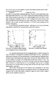
ABSTRACT The structural quality of GaAs layers grown at 200*C by molecular beam epitaxy (MBE) was investigated by transmission electron microscopy (TEM). We found that a high crystalline perfection can be achieved in the layers grown at this low temperature for thickness up to 3 Pam. in some samples we observed pyramid-shaped defects with polycrystalline cores surrounded by microtwins, stacking faults and dislocations. The size of these cores increased as the growth temperature was decreased and as the layer thickness was increased. The upper surface of layers with pyramidal defects became polycrystalline at a critical thickness of the order of 3P m. We suggested that the low-temperature GaAs becomes polycrystalline at a critical thickness either because of a decrease in substrate temperature during growth or because strain induced by excess As incorporated in these layers leads to the formation of misoriented GaAs nuclei, thereby initiating polycrystalline growth. The pyramidal shape of the defects results from a growth-rate hierarchy of the low index planes in GaAs. INTRODUCTION GaAs integrated circuits are typically fabricated on semi-insulating substrates, and active layers on these substrates are formed either by ion implantation or by epitaxial deposition. A number of problems associated with GaAs devices and circuits are attributed to the semiinsulating GaAs substrate. Among these, the most severe is a parasitic coupling between devices called sidegating. A new buffer layer developed for GaAs circuits, which has high resistivity, a large trap density, and a dielectric breakdown strength about ten times that of semi-insulating GaAs, completely eliminates sidegating in GaAs MESFET circuits [1]. This layer is grown by molecular beam epitaxy (MBE) at a substrate temperature of - 2001C using typical Ga and As fluxes for arsenic stable growth at a rate of ljIm/h [1]. Auger electron spectroscopy and analytical electron microscopy measurements reveal that such layers are very As rich, containing about 1 at. % excess As 12-4]. Infrared absorption measurements [21 indicate that there are about 1020 cm 3 neutral As-antisite-related (Asa'*-related) deep levels in as-grown low-temperature (LT) GaAs of which approximately 5xlOi cm 3 are in singly ionized charge state (ASa -related defect) as shown by electron paramagnetic resonance (EPR) studies [4].. A shift inthe (400) xray diffraction peak of LT GaAs as compared with GaAs reveals a 0.1% increase in the lattice parameter consistent with the excess As observed [2,3]. Strain in the LT GaAs was also detected by transmission electron microscopy (TEM) in a study that utilized convergent beam electron diffraction [2]. The TEM studies [2,3] have also shown that LT GaAs layers grown in the temperature range 200-300"C have a high crystalline quality, provided the layer thicknesses are less than 2 p
Data Loading...