The Band Offsets of Isomeric Boron Carbide Overlayers
- PDF / 265,913 Bytes
- 6 Pages / 612 x 792 pts (letter) Page_size
- 80 Downloads / 386 Views
L5.40.1
The Band Offsets of Isomeric Boron Carbide Overlayers A.N. Caruso1, P. Lunca-Popa1,3, Y.B. Losovyj2, A.S. Gunn3 and J.I. Brand3 1 Department of Physics & Astronomy and the Center for Materials Research and Analysis (CMRA) Behlen Laboratory of Physics University of Nebraska, Lincoln, NE 68588-0111 2 Center for Advanced Microstructures and Devices (CAMD), Louisiana State University, Baton Rouge, LA 70806 3 Department of Engineering University of Nebraska-Lincoln Lincoln, NE 68588-0511 ABSTRACT Semiconducting boron carbide overlayers, formed from the decomposition of orthocarborane and metacarborane have been studied by angle resolved photoemission. The incurrence of surface photovoltage and the photovoltaic process, from the photoemission experiment, reveal band offsets in the orthocarborane multilayer configurations that are invereted relative to single layer configurations. Defect induced gap states which trap charge at the heterostructure interface is used as one explanation of these results. The role of defects is also used to help illuminate why opposite semiconducting type materials are formed from the decomposition of isomer carborane molecules. INTRODUCTION Recent experimental results [1,2] demonstrated that boron carbide fabricated from the precursor molecules closo – 1,2 dicarbadodecaborane (orthocarborane) and closo – 1,7 dicarbadodecaborane (metacarborane) form p-type and n-type semiconducting thin films. Based on these results an all boron carbide p-n junction diode [3] was constructed. These “heteroisomeric” diodes also demonstrated both photovoltaic [3,4] and neutronvoltaic [3] responses. The fundamental question arising from this discovery is why thin films composed of isoelectronic molecules, with the same chemical makeup and differing only by carbon position (Figure 1), would form opposite semiconducting types? To begin providing answers to this observed phenomenon, a systematic photoemission study of surface photovoltage and photovoltaic accumulation was completed with boron carbide overlayers. This experiment is a study of the electronic structure created at the metal/semiconductor and semiconductor/semiconductor interface.
Figure 1. (LEFT) closo – 1,2 dicarbadodecaborane or metacarborane and (RIGHT) closo – 1,7 dicarbadodecaborane or orthocarborane. Both molecules are isoelectronic with the constiutients C2B10H12.
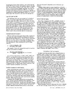
L5.40.2
Figure 2. Photoemission based rectification of p-type (a) and n-type (b) semiconductors through the accumulation of surface photovoltage. The dotted lines represent the final band position upon rectification. The initial band bending is caused by the space charge layer at the vacuum interface. EXPERIMENTAL DETAILS The electronic structure studies were undertaken by angle resolved photoemission. Photoemission extracts a quantity which is proportional to the electron density of states (photoemission intensity) as a function of binding energy; we treat the Fermi level as zero binding energy. The photoemission experiments were completed at the Center for Advanced Microst
Data Loading...