The growth of Cu-Sn intermetallics at a pretinned copper-solder interface
- PDF / 3,998,348 Bytes
- 10 Pages / 630 x 792 pts Page_size
- 84 Downloads / 240 Views
I.
INTRODUCTION
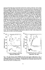
S O L D E R I N G is commonly used to join components in electronic packaging. The most widely used solder system is Pb-Sn, and the most common substrate metal is copper. The Pb-Sn solder bonds to Cu by forming a layer of Cu-Sn intermetallic at the wetted interface. ~1-4] The solderability of a Cu substrate depends on the ease with which the intermetallic can form, and the reliability of the joint is influenced by the integrity of the intermetallic layer. When Cu is exposed to air, it develops an oxide layer that must be removed, usually by applying a reactive flux, before it can bond to solder. To eliminate this problem, the copper lands on printed circuit boards are commonly "pretinned" by coating with a thin layer of solder, t5,6,71 However, the solderability of the pretinned surface often deteriorates during storage or hightemperature baking prior to final processing. For example, Figure 1 shows the effect of baking at 170 ~ on a copper land that was pretinned with -~10 /xm of eutectic solder (63Sn-37Pb). The surface and cross-sectional views of the original configuration show a typical microstructure in which the solder contains primarily eutectic constituent with some Pb dendrites, and the surface is coated by a thin layer of Cu-Sn intermetallic. During
A.J. SUNWOO, formerly with the Lawrence Berkeley Laboratory, Berkeley, CA, is Materials Engineer, Lawrence Livermore National Laboratory, Livermore, CA 94550. J.W. MORRIS, Jr., Professor of Metallurgy, is with the Department of Materials Science and Mineral Engineering, University of California, Berkeley, CA 94720. G.K. LUCEY, Jr., Chief of Producibility Technology Branch, is with the United States Army's Harry Diamond Laboratories, Adelphi, MD 20783. Manuscript submitted May 24, 1991. METALLURGICAL TRANSACTIONS A
baking, the Pb withdraws from the surface into isolated islands, and the intermetallic grows to penetrate between, leading to an interface with poor solderability.[8] The loss of solderability of pretinned joints has been a troublesome problem for the electronics industry. The bulk of research on intermetallic growth in Cu-solder joints has concentrated on growth into relatively thick solder layers. I1-4,9!While this work has helped to clarify the growth behavior of the intermetallic phases, growth in pretinned joints is complicated by the finite quantity of available tin and by the possibility of Pb reconfiguration at the free surface. The present work was undertaken to study this behavior, with particular emphasis on the mechanisms of intermetallic growth that cause intermetallic penetration at the free surface.
II.
BACKGROUND
Since Cu and Pb are almost immiscible, the PbSn-Cu ternary system can be largely understood on the basis of the Pb-Sn and Cu-Sn binary phase diag r a i n s , [10"11'12l which are shown in Figure 2. The addition of Cu decreases the eutectic temperature of Pb-Sn by only 2 ~ from 183 ~ to 181 ~ ~12j and the solubility at the eutectic point is only 0.23Cu [131(all compositions will be given in weight percen
Data Loading...