The influence of Ti and TiN on the thermal stability of CoSi 2 .
- PDF / 196,587 Bytes
- 6 Pages / 612 x 792 pts (letter) Page_size
- 34 Downloads / 320 Views
The influence of Ti and TiN on the thermal stability of CoSi2. C. Detavernier, Department of Solid State Sciences, Ghent University, Krijgslaan 281/S1, B-9000, Gent, Belgium
Guo-Ping Ru, Department of Electronic Engineering, Fudan University, Shanghai, 200433, China
R.L. Van Meirhaeghe Department of Solid State Sciences, Ghent University, Krijgslaan 281/S1, B-9000, Gent, Belgium
K. Maex IMEC, Kapeldreef 75, B-3001 Leuven, Belgium. also at E.E. Dept, K.U. Leuven, B-3001 Leuven, Belgium.
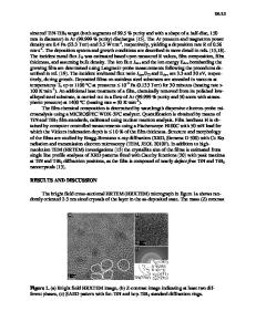
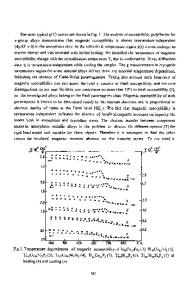
ABSTRACT In this work, AFM and sheet resistance measurements are used to characterize the thermal stability of thin CoSi2 films. We were particularly interested in the influence of different multilayer structures on the topography and surface roughness. Four different multilayer structures (Co/Si, TiN/Co/Si, Ti/Co/Si and Co/Ti/Si) were investigated. Thermal degradation of CoSi2 formed from a standard Co/Si structure is found to have an activation energy of about 4.2 eV, independent of layer thickness (in agreement with previous results by Alberti et al.). A TiN capping layer is shown to improve the thermal stability. However, if the TiN layer is too thick (e.g. 50 nm), a new failure mode is observed : although the TiN prevents grain boundary grooving of the silicide, the thermal stress induced by the TiN causes the CoSi2 layer to crack. For a Ti capping layer, a strong increase of the thermal stability of the CoSi2 layer is observed, even if the Ti capping layer is removed by a selective etching step after the first RTP annealing. The presence of a very thin Ti-O-N containing layer on the CoSi2 surface seems to strongly decrease surface diffusion and in this way reduce the tendency for grain boundary grooving.
INTRODUCTION In the self-aligned silicide (SALICIDE) process, the formation of the silicide layer requires the consumption of silicon from the substrate. In deep sub-micron CMOS devices, the junction depth is scaled down to only tens of nanometers. Since the formation of a thick silicide layer would ultimately consume the entire junction, the silicide thickness has to be reduced simultaneously with the junction depth. Unfortunately, thin silicide films are more likely to agglomerate. Therefore, characterization of the thermal stability of thin silicides and the prevention from agglomeration have attracted much attention recently [1-6]. Measuring the sheet resistance is a common method to characterize thermal agglomeration. Although a low sheet resistance is one of the main priorities of the application engineers, the K6.7.1
sheet resistance measurement as such does not provide any details about the nature of the deterioration process (islanding, grain boundary grooving, cracking, …). From a scientific point of view, measuring surface roughness, an important feature of surface topography, can be considered more appropriate to characterize thermal agglomeration. Recently, scanning tunneling microscopy (STM) and its extensions have become powerful tools for real-space surface imaging with high resolution in three dimensions.
Data Loading...