The mechanism of sputter-induced epitaxy modification in YBCO (001) films grown on MgO (001) substrates
- PDF / 495,765 Bytes
- 11 Pages / 612 x 792 pts (letter) Page_size
- 68 Downloads / 311 Views
MATERIALS RESEARCH
Welcome
Comments
Help
The mechanism of sputter-induced epitaxy modification in YBCO (001) films grown on MgO (001) substrates Y. Huang, B. V. Vuchic, M. Carmody, P. M. Baldo, and K. L. Merkle Materials Science Division, Argonne National Laboratory, Argonne, Illinois 60439
D. B. Buchholz, S. Mahajan, J. S. Lei, P. R. Markworth, R. P. H. Chang, and L. D. Marks Department of Materials Science and Engineering, Northwestern University, Evanston, Illinois 60201 (Received 9 July 1997; accepted 25 January 1998)
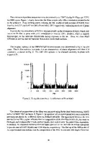
The sputter-induced epitaxy change of in-plane orientation occurring in YBa2 Cu3 O72x (001) thin films grown on MgO (001) substrates by pulsed organo-metallic beam epitaxy (POMBE) is investigated by a series of film growth and characterization experiments, including RBS and TEM. The factors influencing the orientation change are systematically studied. The experimental results suggest that the substrate surface morphology change caused by the ion sputtering and the Ar ion implantation in the substrate surface layer are not the major factors that affect the orientation change. Instead, the implantation of W ions, which come from the hot filament of the ion gun, and the initial Ba deposition layer in the YBCO film growth play the most important roles in controlling the epitaxy orientation change. Microstructure studies show that a Bax Mg12x O buffer layer is formed on top of the sputtered substrate surface due to Ba diffusion into the W implanted layer. It is believed that the formation of this buffer layer relieves the large lattice mismatch and changes the YBCO film from the 45± oriented growth to the 0± oriented growth.
I. INTRODUCTION
Grain boundary junctions in high-Tc superconductor materials have attracted much attention in recent years. Many methods have been developed to fabricate grain boundary junctions (GBJ’s). Among others, the step edge method,1,2 bicrystal method,3–5 and biepitaxy method6,7 have been extensively studied. Junctions made by the bicrystal method are presently being used in commercial devices. The disadvantage of these fabrication processes is that they are all quite complex and/or expensive. Therefore there is a need for simpler and inexpensive procedures. The method to be discussed in this paper is similar to but much simpler than the biepitaxy technique. This method uses low-energy ion sputtering to selectively treat the substrates. Under specific synthesis conditions the superconductor films grow with different in-plane orientations on the sputtered and nonsputtered substrate areas and thus form GBJ’s between the two areas. The change of epitaxy orientation by ion sputtering will be termed “sputter-induced epitaxy modification” (SIEM) and the method to form GBJ’s by this change, the SIEM method. The SIEM phenomenon was first observed by Chew et al.8 They grew c-axis normal YBa2 Cu3 O72x (YBCO) films on MgO (001) substrates by the coevaporation method. On nonsputtered substrates they observed the inplane orientation relation to be [100]YBCOyy[100]MgO , but on s
Data Loading...