Thermal Studies on Stress-Induced Void-Like Defects in Epitaxial-CoSi 2 Formation
- PDF / 2,798,977 Bytes
- 8 Pages / 417.6 x 639 pts Page_size
- 99 Downloads / 341 Views
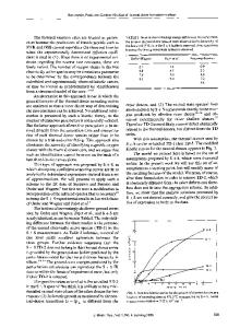
ABSTRACT We report experimental findings on the thermal-induced stress-voiding observed during epitaxial CoSi- formation on patterned Si(100) wafers associated with the Co/Ti-interposing layer scheme [1-6]. The first rapid thermal process (RTP) in a typical SALICIDE process was studied by varying the temperature and the RTP ramp-up rate. Based on ex-situ cross-sectional transmission electron microscopy (XTEM), crystal defects were observed at shallow trench isolation (STI)/Si and gate spacer/Si edges after annealing at temperatures greater than 520'C. In addition, isothermal anneals for various time periods resulted in increased encroachment of an ultra-thin CoSi2 -phase at the STI/Si edge. Higher temperature anneals also resulted in a corresponding increase in void size. In addition, higher ramp-up rates led to a thicker CoSi2 "pocket" film at the tensile-stressed STI/Si edge, aligned epitaxially along the I11I-habit planes. Our attempts to bypass the CoSi formation in order to alleviate the anomalous Si diffusion was found to be irrelevant to the voiding issue, due to the inherent nature of this film stack system to nucleate CoSi2 as the first phase. By comparing our experimental observations of voiding with Hu's analysis of the trench isolation stress fields, we found good agreement with the predicted stress field distribution in the active Si and STI/Si edge with the locations of void nucleation. The anomalously large stress induced is still not known, but can be attributed to the encroaching CoSi, film which tends to realign epitaxially along the STI/Si interface.
INTRODUCTION Epitaxial CoSi 2, fabricated using the Co/Ti-interposing layer scheme, first proposed by Yang et al. on Si(l 11)[1] and Wei et al. on (100)Si [2], have been extensively studied over the past decade in view of its prospects as a potential SALICIDE (self-aligned silicide) candidate, due to its potential ease of integration in a typical CMOS/BiCMOS fabrication process flow. One of its attractiveness over the conventional polycrystalline films is its single-grain nature and the inherent sharp interfacial uniformity on silicon. This has a huge advantage, especially in terms of preserving the silicided ultra-shallow junction (]1l00A) sandwiched between oxide masks also led to the observation of defect generation under the silicide film [9]. In all of the reports thus far, none has focused on clarifying the voiding observed in the Co/Tiinterposing layer scheme, although Byun et al. [3] did attribute the anomalous Si-diffusion to the TiSi and CoSi formation. We will discuss their report in greater depth. Steegen el al. had provided a good physical picture into the silicide-induced stress at film edges based on FEM analysis (finite element method) incorporating plane-strain approximation [1 0]. However, based on these FEM simulations, the film stress of epitaxial CoSi 2 has been predicted to be only twice that of its polycrystalline counterpart and comparable to that of TiSi 2 [11]. Bearing in mind the possible inaccuracies in the simplifying as
Data Loading...