Thermo-Electrical Analysis of an Optoelectronic Modulator Integrated in a SOI Rib Waveguide Operating in the Gb/s Regime
- PDF / 625,276 Bytes
- 6 Pages / 612 x 792 pts (letter) Page_size
- 79 Downloads / 301 Views
0934-I10-02
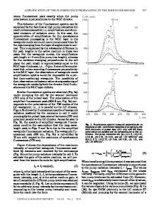
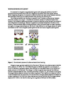
Thermo-Electrical Analysis of an Optoelectronic Modulator Integrated in a SOI Rib Waveguide Operating in the Gb/s Regime Mario Iodice, Giuseppe Coppola, and Rocco Cristian Zaccuri Istituto per la Microelettronica e Microsistemi, Consiglio Nazionale delle Ricerche, Via Pietro Castellino 111, Napoli, 80131, Italy ABSTRACT Silicon is the most diffused material for microelectronic industry and, in recent times, it is becoming more and more widespread in integrated optic and optoelectronic fields. We present the thermo-electro-optical analysis of an integrated waveguide-vanishing-based optical modulator based on free-carrier dispersion effect, realizable on standard SOI wafer. The optical behavior is based on the vanishing of the lateral confinement in the rib region, and consequent cut-off of the propagating mode. Results show that an optical modulation depth close to 100% can be reached with a bandwidth of about 154 MHz. Smart electrical driving, that is an injection overdrive of a few volts for a very short time, allows to reach total ON-OFF switching time of about 860 ps. For that bias scheme the fall transient is then limiting the whole dynamic and the resulting bit rate in a pure digital modulation scheme is about 1.2 Gb/s. INTRODUCTION We describe in this paper a new type of optoelectronic modulator integrated in a SOI waveguide, fully compatible with the standard CMOS manufacturing technology. The main feature of the proposed modulator is the planarity, that is the absence of steps or ribs in the active region of the modulator, i.e. the region where is achieved the interaction with the optical beam. In this paper we report a detailed description both of the modulator structure and its optical and electrical behavior. The fabrication process-flow and the coupled thermoelectrical behaviour are analyzed by SILVACO International [1] complementary software, in particular with the aim to investigate the thermal contacts impact of the internally generated heat on the optical characteristics, both in static and dynamic conditions. 3 mm All optical analyses were performed by RSoft complementary software [2]. In our simulations the n+ ~1 mm p+ complete influence of the temperature distribution on 3 mm the optical behavior is taken in account. In particular, epilayer nSiO2 the effect of the temperature on the non-uniform distribution of the injected free carriers is modeled. A (0.5 mm) first proposed device exhibits a modulation depth (≈ substrate 100 %) and an operation frequency (≈ 30 MHz) Figure 1. (a) sketch of the modulator structure suitable for several applications. In order to optimize and (b) active region cross section. the device, we have considered the possibility to incoming waveguide
Anode contact
Wafer surface
outcoming waveguide
Cathode contact
SiO2 layer
Ep ilay er bst rat e
Su
active area
shrink the structure transverse section to 1×1 µm2–wide active region, reporting differences and performance improvement of the new configuration in comparison with results reported before. Maintain
Data Loading...