Thermoplastic Deformation and Residual Stress Topography of 4H-SiC Wafers
- PDF / 792,713 Bytes
- 6 Pages / 612 x 792 pts (letter) Page_size
- 82 Downloads / 315 Views
J6.2.1
Thermoplastic Deformation and Residual Stress Topography of 4H-SiC Wafers Robert. S. Okojie1 Ming Zhang2 1 2
NASA Glenn Research Center, 21000 Brookpark Road, M/S 77-1, Cleveland, OH 44135, USA Department of Materials Science & Engineering, CWRU, Cleveland, OH 44106, USA
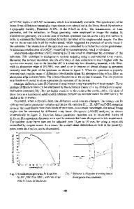
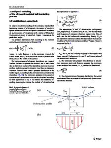
ABSTRACT We have measured thermoplastic deformation in as-received, single-side polished, 4H-SiC wafers and also residual stresses in homoepitaxially grown epilayers on wafers by radius curvature measurements. The wafers studied had n-type resistivities of 0.010-0.011 Ω-cm and p-type resistivities of 4.42, 4.72, 9.57 Ω-cm. In a first thermal excursion to 900 oC in vacuum, the bow height of the bare substrates in all cases decreased with temperature. Upon cooling down, however, the bow heights remained largely unchanged from their values at 900 oC. A second cyclic excursion to 900 oC did not yield any significant change in the curvature, thus indicating that the substrates had thermoplastically deformed in the first heating cycle. Epilayers having nitrogen doping between 5 x 10¹⁷ and 2 x 1019 cm-3 grown on the n- and p-type substrates resulted in compressive stresses ranging between 190 and 400 MPa in the epilayers. Transmission electron microscopy (TEM) examination of the n-type epilayer (with doping levels of 5 x 1017 cm-3 and 5 x 1018 cm-3) on the n-type substrate, revealed bands of stacking faults (SFs) confined within the epilayers after the bicrystals were further annealed at 1150°C in nitrogen for thirty minutes. These doping levels are approximately one and two orders of magnitude below the reported threshold value of 3 x 1019 cm-3 previously suggested for the onset generation of SFs in annealed n-type 4H-SiC epilayers. The calculated residual stresses in all the epilayers were above the critical stress for the motion of dislocations above 1000 °C in 4H-SiC. Thus the SFs that form by glide of pre-existing partial dislocations may actually be stress induced and occur across a much wider range of doping levels. Therefore, it is possible that a significant mechanism for formation of the stacking faults and 3C bands observed in thermally treated 4H-SiC wafer is stress relief via the generation and motion of new and pre-existing partial dislocations on the basal planes of 4H-SiC. INTRODUCTION The deleterious effects of internal stresses on the yield and reliability of semiconductor electronic devices continue to remain a major research topic [1]. In silicon carbide (SiC) technology, the production of bulk crystals for high volume commercialization is primarily motivated by the advantages provided by the superior electronic properties of this material (i.e., high breakdown field, wide bandgap, and high thermal conductivity) over traditional semiconductors [2]. These properties will allow SiC-based devices to support high speed and high voltage switching, and to operate in much higher temperature and radiation environments than conventional semiconductor devices. However, the magnitude of stresses that develop during bulk growth of single
Data Loading...