Thick Films for Dielectric Isolation by Lateral Epitaxy from the Melt
- PDF / 6,135,491 Bytes
- 11 Pages / 417.6 x 639 pts Page_size
- 41 Downloads / 215 Views
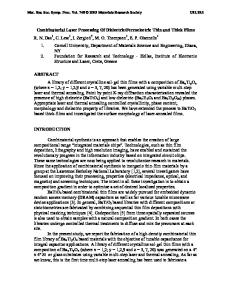
THICK FILMS FOR DIELECTRIC ISOLATION BY LATERAL EPITAXY FROM THE MELT G. K. CELLER AND L. E. TRIMBLE AT&T Bell Laboratories, Murray Hill, New Jersey 07974 ABSTRACT Dielectric Isolation (DI) technology has been available for almost twenty years. It was first developed for low capacitance, high speed circuits, and was later adapted to radiation hardened devices and for high voltage isolation. We describe a new method of forming DI structures that simplifies wafer fabrication, reduces the density of process induced defects, and may lead to a more flexible device design. Our process is based on recrystallization from the melt of thick Si films deposited over oxidized Si wafers, with a regular array of seeding windows opened in the isolation oxide. The recrystallized films are free of grain boundaries and subboundaries. INTRODUCTION In recent years there has been much research aimed at fabrication of high quality thin Si films on SiO [1]. In contrast, thick Si films on SiO 2 were first demonstrated about 20 years ago i2], and have been commercially produced for many years. The process of making dielectrically isolated (DI) wafers consists of several steps. First, (100) Si wafers are V-grooved to a depth of -50 Am by anisotropic etching and oxidized to form a dielectric isolation layer. A very thick layer of -500 am of polysilicon is then deposited by a high temperature CVD process over the oxide to form a new mechanical support or "handle". Once this is accomplished, 80-90% of the initial crystalline substrate is mechanically removed, as shown schematically in Fig. 1. Only small, device-size segments of the original single crystalline wafer remain embedded in the polysilicon handle, electrically isolated from it and from each other. This procedure, developed and perfected over the years, is expensive and includes grinding and lapping steps that are difficult to control and automate. Nevertheless, this is still the only proven technique for obtaining dielectrically isolated thick film structures and the only commercial process for fabricating crystalline Si films of any thickness on the SiO 2. We have recently proposed an alternative to conventional DI technology that is potentially simpler and less expensive [3-51. This method of Lateral Epitaxial Growth over Oxide (LEGO) results in crystalline Si dielectrically isolated from a single crystalline substrate. The absence of the polysilicon handle eliminates the problem of wafer deformation caused by volume changes in polysilicon [6]. In this paper we describe the LEGO method of forming crystalline films isolated from the substrate, its advantages and the remaining problems. The process is based on controlled melting and recrystallization of thick Si films in a special lamp furnace [7]. SAMPLE PREPARATION Samples for crystallization are prepared by oxidation, photolithography, and deposition of polysilicon and Si0 2 films. (100) starting wafers are cleaned and oxidized in a steam ambient to form the dielectric isolation barrier. The oxide is patterned by photolithography t
Data Loading...