Thin Film Stresses in TiW/AlCuSi/TiW Sandwich Structures
- PDF / 292,925 Bytes
- 5 Pages / 420.48 x 639 pts Page_size
- 29 Downloads / 376 Views
THIN FILM STRESSES IN TiW/AlCuSi/TiW SANDWICH STRUCTURES ITON WANG Circuit Technology Group, Santa Clara, CA 95051
Hewlett Packard Company,
5301 Stevens Creek Blvd.,
ABSTRACT
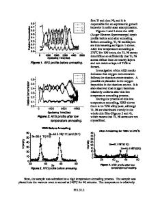
A highly reliable metallization for high current bipolar integrated circuits was developed with the aid of thin film stress analysis to optimize the process. The final structure was a sandwich layer of TiW and AlCuSi alloy. Film stresses were measured for individual TiW layers as well as for the sandwich layers of TiW/AlCuSi/TiW. In this paper, it will be shown how sputter deposition pressure can drastically affect film stress. For individual TiW layers, the film stress can be varied between compressive and highly tensile by adjusting the Argon pressure. Meanwhile, the AlCuSi layers were always tensile under the normal range of sputtering pressures. By controlling the individual film stresses, a sandwich layer can be designed so that the overall structure has a very low average stress. This work will also show how a TiW capping layer has a major effect on the final average stress of the sandwich structure.
INTRODUCTION
In order to improve performance as well as to increase packing density, it has become necessary to use multilevel metallizations. The universal trend toward using diffusion barriers [1,2] and planarization techniques [3] has created a nightmare for the thin film engineer. Some very complex structures are being used to improve device performance and yield. Processes such as CVD tungsten [4] and metal pillars [5] are being developed for contact and via fills. Planarization schemes include oxide etch-back, polyimide, SOG, BPSG reflow, BSQ and hot substrate metal depositions. All these processes go through some temperature cycling and create an interfacial layer which can and usually does generate stress. If these stresses are not controlled, device degradation or failure can occur. It is therefore important to understand the potential problems that can be caused by thin film stresses. The impact of the substrate on stress measurements [6) should not be overlooked. Ionic Systems did a study comparing prime silicon wafers with test or monitor grade wafers and found the measured values of stress to vary by an order of magnitude. Based on test results using a single point measurement at the center of the wafer, the following recommendations were made: 1. For the greatest accuracy and repeatability, only prime silicon wafers should be used for stress measurements. 2. Prime wafers that do not have initial readings in the main grouping should be discarded. Other tests have shown that the crystal orientation of silicon wafers can have a major effect on the magnitude and polarity of stresses measured. This is not to imply that the quality of the wafer or its orientation affects film stress, but the accuracy of measurement depends on measurement techniques. In systems such as the Canon LSF-500 or Ionic Systems' Stressgauge, the property being measured is the bow of the wafer or substrate. The deflection in the wafer is primarily due to
Data Loading...