Towards p-type doping of ZnO by ion implantation
- PDF / 353,614 Bytes
- 6 Pages / 612 x 792 pts (letter) Page_size
- 22 Downloads / 416 Views
B8.7.1
Towards p-type doping of ZnO by ion implantation V. A. Coleman1, H. H. Tan1, C. Jagadish1, S. O. Kucheyev2, M. R. Phillips3 and J. Zou4 1 Department of Electronic Materials Engineering, The Australian National University, Canberra, ACT 0200, Australia 2 Lawrence Livermore National Laboratory, Livermore, CA 94550, U.S.A. 3 Microstructural Analysis Unit, University of Technology Sydney, Broadway, NSW 2007, Australia 4 School of Engineering and Centre for Microscopy and Microanalysis, The University of Queensland, St Lucia, QLD 4072, Australia
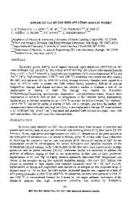
ABSTRACT Zinc oxide is a very attractive material for a range of optoelectronic devices including blue light-emitting diodes and laser diodes. Though n-type doping has been successfully achieved, p-type doing of ZnO is still a challenge that must be overcome before p-n junction devices can be realized. Ion implantation is widely used in the microelectronics industry for selective area doping and device isolation. Understanding damage accumulation and recrystallization processes is important for achieving selective area doping. In this study, As (potential p-type dopant) ion implantation and annealing studies were carried out. ZnO samples were implanted with high dose (1.4 x 10¹⁷ ions/cm2) 300 keV As ions at room temperature. Furnace annealing of samples in the range of 900oC to 1200oC was employed to achieve recrystallization of amorphous layers and electrical activation of the dopant. Rutherford backscattering/channeling spectrometry, transmission electron microscopy and cathodolumiescence spectroscopy were used to monitor damage accumulation and annihilation behavior in ZnO. Results of this study have significant implications for p-type doing of ZnO by ion implantation.
INTRODUCTION Zinc Oxide (ZnO) is increasingly attracting more and more interest as a material for a range of optoelectronic devices including blue and UV light-emitting diodes and laser diodes [1]. With a large exciton binding energy of 60 meV at room temperature, a wide band gap of 3.4 eV [1] and resistance to radiation damage [2], it is the perfect candidate for such devices. Devices incorporating a p-n junction have yet to be realized, however, because p-type doping of ZnO is still proving to be a major challenge [3]. Currently, there is still much to be understood about the issues of dopant incorporation and activation in ZnO [4]. Ion implantation is widely used in the microelectronics industry for selective area doping and device isolation [5]. Ion implantation of potential p-type dopants [6] and co-implantation studies [7] are beginning to show promising results for producing p-type ZnO. A thorough understanding of damage accumulation and recrystallization processes is thus important for
B8.7.2
achieving consistent and controllable selective area doping. In this study, we address some of these issues by monitoring the damage accumulation and annihilation behavior in single crystal ZnO that has been implanted with very high-doses. We have chosen to conduct the high-dose implants with arsenic io
Data Loading...